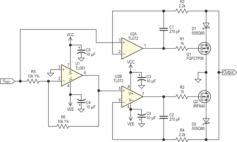
For symmetrical applications, the circuit of Figure 4 works well. It is made up of the positive limiter already seen and a complementary negative limiter connected in parallel. A single positive reference voltage is used to control both voltage limits. The negative reference voltage is generated by a unity gain inverter, U1.
 |
|
| Figure 4. | Schematic for a symmetrical shunt voltage limiter. |
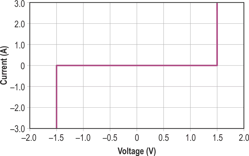
Static measurements are in Table 2 and Figure 5 is the corresponding graph. Figure 5 shows symmetrical voltage limiting.
| Table 2. | Measurements taken for the circuit in Figure 4 |
||||||||||||||||||||||||||||||||||||||
|
|||||||||||||||||||||||||||||||||||||||
 |
|
| Figure 5. | Curve for circuit in Figure 4, limiting voltage is very symmetrical about 0 V. |
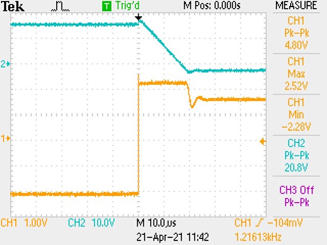
Since the op amp is in saturation when the circuit output voltage is below the limit, the response is slow. In Figure 6, a square wave was provided by a generator set to produce an open circuit peak to peak voltage of 4 V. The generator has 50 ohms output impedance. The oscilloscope CH1 is the circuit output voltage and CH2 is the op amp output. It takes about 20 µs for the op amp to slew 20 volts from approximately +15 V to –4 V.
 |
|
| Figure 6. | Waveforms for circuit in Figure 4, shows slewing is the major limit to response. See text for details. |
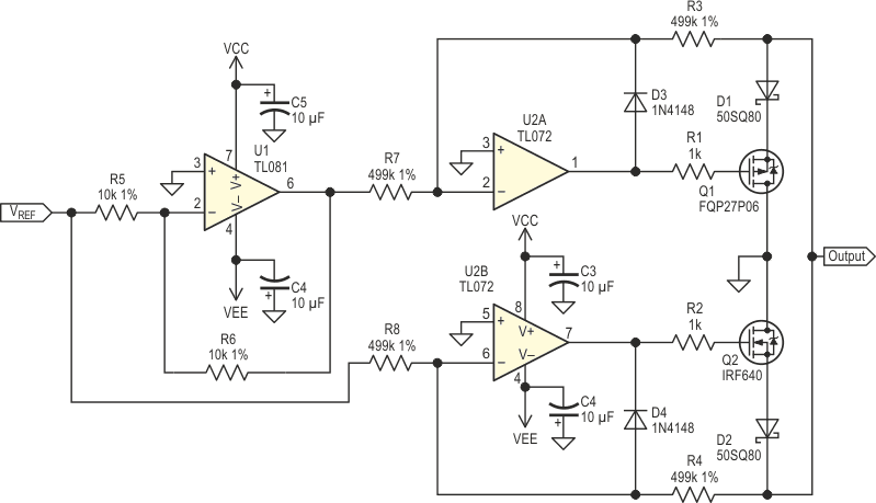
An improved circuit which does not saturate the op amp is in Figure 7. The main op amps U2A and U2B are now unity gain inverting amplifiers. Diodes D3 and D4 limit the op amps output voltage to 0.7 V in saturation [7]. Op amp U2A output now has to slew only from +0.7 V to –4 V. Since the input resistor R3 will load the output, it is selected to be twice the minimum acceptable resistance specified of 200 kΩ, I had 499k 1% resistors on hand, so I used those. Waveforms are taken using only the positive limiter part from Figure 7, with 200k resistors for R3 and R7.
 |
|
| Figure 7. | Schematic symmetrical shunt voltage limiter with the final op-amps operated in inverting mode. |
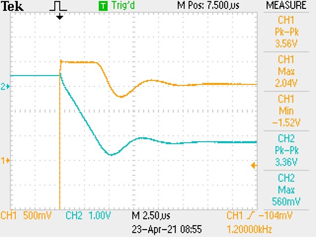
In Figure 8, oscilloscope CH1 is the circuit output voltage and CH2 is U2A output. The response is 5 µs, about four times faster than with the initial circuit.
 |
|
| Figure 8. | Response time for circuit in Figure 7, bounded voltage leads to shorter slewing time. See text for details. |
Table 3 and Figure 9 outline static measurements very similar to the first circuit, except that the current below VREF is in the microamperes range. To have asymmetrical limiting, remove the inverter stage and use two reference voltage sources.
| Table 3. | Measurements taken for circuit in Figure 7 |
||||||||||||||||||||||
|
|||||||||||||||||||||||
 |
|
| Figure 9. | Curve for positive half only of circuit in Figure 7, increased speed does not affect DC performance. |
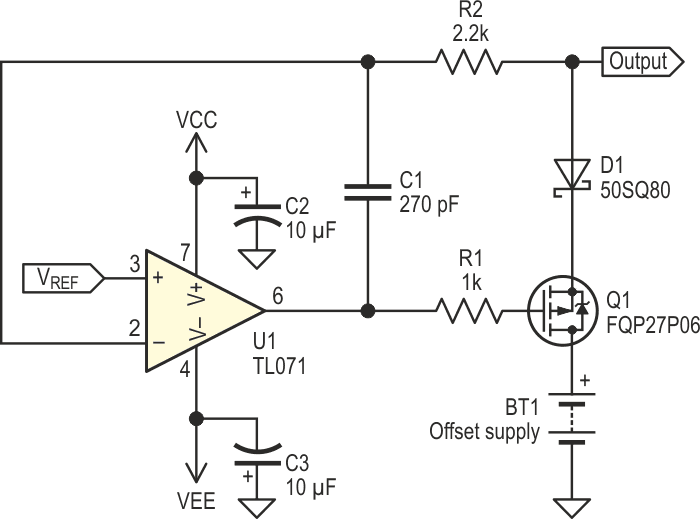
If you need to limit the voltage to a value lower than 700 mV, the voltage lost in the diode will make it almost impossible to meet that requirement with either circuit. But if you connect the P-channel MOSFET drain to a negative voltage source, then any voltage limit is possible even 0 V. The same approach can be used for the N channel MOSFET. The circuit in Figure 10 does just that with performance comparable to the circuits above. The offset voltage source, battery B1 in schematic, should be capable of supplying the required current.
 |
|
| Figure 10. | Schematic of a voltage limiter capable of operating below 1 V. |
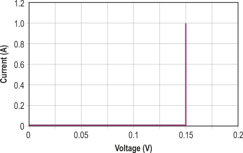
Table 4 gives the results with a 150-mV reference and an offset power supply of 1.8 V. Current versus voltage curves at high current, up to 1 A, are graphed in Figure 11. Here again the circuit shows sharp knee, low leakage and constant limiting voltage. The same technique can be used with the schematic in Figure 7. For limiting voltage values below approximately 1 V, error budget calculations should govern your selection for the op amps offset voltage and bias current maximum values.
| Table 4. | Measurements taken for circuit in Figure 10 |
||||||||||||||||||||
|
|||||||||||||||||||||
 |
|
| Figure 11. | Curve for circuit in Figure 10. |
This circuit could be used as a teaching aid, set the limit voltage to zero and insert the circuit in a test circuit for students. Imagine the fun and puzzlement of having a short circuit for one ohmmeter polarity and an open circuit for the opposite polarity!
For best results in high current applications, the voltage limiter should be installed between the voltage source and the device to be protected.
I tested various diodes: Zener, silicon PN, Schottky barrier and LEDs, and none of these have such a sharp knee, low leakage and can carry as much current or are as flexible in use as the above circuits.
With simple modifications, the clamping voltage could be extended to higher values, but that is another design idea.
References
- Peter Demchenko, Shunt circuit clips large transients or regulates voltage.
- Chris Toliver, High-power shunt regulator uses BJT & reference IC.
- Adolfo Mondragon, Power Zener using the LM317
- Stuart R. Michaels, MOSFET shunt regulator substitutes for series regulator.
- Robert N. Buono. High-Current, Low-Voltage Shunt Regulator.
- Sansen, Willy. M. Analog Design Essentials. ISBN-13: 9781489978912, page 24.
- Pease, Robert. «Bounding, clamping techniques improve circuit performance». EDN, November 10, 1983. Pages 277 to 289.