I need a circuit to limit the voltage across some dissipation limited devices. It must: limit the voltage to a maximum of 1.5 V, have symmetrical limiting, be capable of accepting a current of 2 A, and leak less than 100 µA at 1 V.
Two Zener diodes in series, anode to anode, would do the trick, but Zener diodes with VZ = 0.8 V and a 2 W dissipation are not commercially available.
I searched the web to find what was available. In EDN’s design ideas webpage, I found one [1], however the circuit cannot limit voltages lower than 2.5 V. In another design idea [2] again, the minimum voltage of 1.8 V is too high for my application, but the current goes up to 6 A. Another reference [3] uses a single part that limits at 1.5 V, but its resistance is about 1 Ω and that combined with my requirement of 2 A will give too high a voltage. Another circuit [4] depends on the MOSFET characteristics to set the limit voltage and in my application that is not an option as I would have to test and select MOSFETs to find acceptable limit voltages. Finally, [5] offers a voltage range that is perfect with a maximum current of 8 A, but the off current is 200 µA and this is twice my limit. In conclusion: I have to design a circuit to suit my needs.
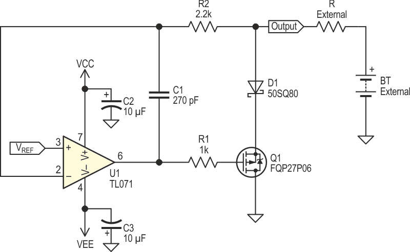
The circuit of Figure 1 has the needed characteristics. It is a modified shunt type voltage regulator. In this application, the voltage to be regulated comes from an external source, battery BT, in the schematic.
 |
|
| Figure 1. | Schematic of a simple positive shunt voltage limiter. |
Let’s say that the reference voltage, VREF in the schematics, is 1.5 V and that the voltage at the circuit output is also 1.5 V. Since both inputs to U1 are the same, the op amp output is 0 V, the MOSFET is off and no current flows through it. If the external voltage rises, the op amp output will become more negative and turn on Q1, a P-channel MOSFET, used in a source follower configuration, and more current flows in D1 and Q1. When the circuit is limiting, the impedance seen at the output is approximately the sum of the diode resistance plus Q1’s RDS(ON) divided by the open loop voltage gain of U1. The output impedance is in the hundreds of milliohms range. Resistor R1 is a gate stopper resistor to eliminate the risk of oscillations in the MOSFET.
When the output voltage goes lower than the reference voltage, U1 output will rise positive and Q1 will enter the weak-inversion or subthreshold region [6]. The feedback loop then becomes open and the op amp will saturate to the most positive voltage it can supply. Diode D1, blocks any reverse current that would flow through Q1’s body diode if the voltage at the output terminal goes negative. With the voltage at the output is below the limiting voltage, the current that flows in the circuit output is the sum of D1 reverse leakage and U1 input bias current.
Resistor R2 protects U1 in case of a negative overvoltage and allows loop compensation to take action via C1 by isolating the op amp inverting input from the output. The value of C1 is dependent on the op amp, the MOSFET and the layout.
Maximum rated current is defined as the current that makes the total voltage drop across the diode and the MOSFET equal to the reference voltage. The equation is:
Where VREF is the reference voltage, VF is the voltage drop across D1 at the rated current, RDS(ON) is the MOSFET maximum drain-source resistance and IMAX is the maximum current available from the source. If more current than IMAX is applied, the output voltage rises linearly from the set limit. If too high a current is applied, either D1 or Q1 will overload or overheat, resulting in permanent failure. Depending on the MOSFET used, maximum current can also be limited by the op amp maximum output voltage.
Actual measurements are listed in Table 1. All measurements were taken with a VCC of +15.5 V and a VEE of –15.5 V because those are the target instrument supply voltages. To get good results, care should be taken as to where the voltmeter is connected during measurements; a four wire Kelvin connection and a stable reference voltage source are a must.
| Table 1. | Measurements taken for the circuit in Figure 1 |
||||||||||||||||||||||||||
|
|||||||||||||||||||||||||||
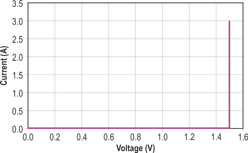
An current versus voltage curve for circuit in Figure 1 is shown in Figure 2. The circuit holds the voltage to within 1 mV of the reference while the current varies from 3 µA to 3 A. The knee is very sharp.
 |
|
| Figure 2. | Current versus voltage for circuit in Figure 1, high current, note the square knee. |
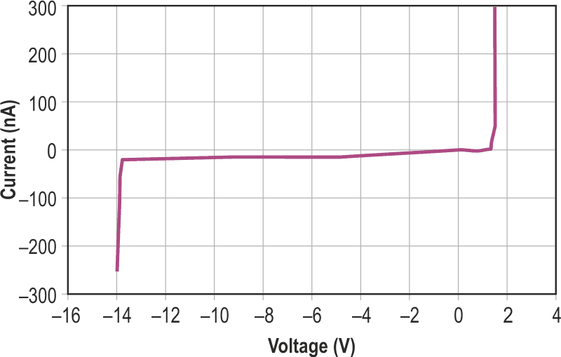
In Figure 3, the low current portion of the curve is shown; the total current range is almost 170 dB. The current is below 100 nA for most of the range between –14 V and +1.5 V. We can see that when the voltage reaches negative 14 V, current increases. The increase in current is because the voltage is getting close to the common voltage range limit for this op amp.
 |
|
| Figure 3. | CCurrent versus voltage for circuit in Figure 1, low current, showing current increase when nearing common mode range limit. |
The circuit uses commonly available parts. Diode D1 and MOSFET should be selected to carry the full current and have a total voltage drop less than the reference voltage at the maximum current. Depending on the current value, the MOSFET may need heatsinking. I used a Schottky diode for D1, but a silicon p-n diode would do also. Since the input bias current of U1 flows from the output, I used a JFET input op amp; any low bias current op amp will work.
References
- Peter Demchenko, Shunt circuit clips large transients or regulates voltage.
- Chris Toliver, High-power shunt regulator uses BJT & reference IC.
- Adolfo Mondragon, Power Zener using the LM317
- Stuart R. Michaels, MOSFET shunt regulator substitutes for series regulator.
- Robert N. Buono. High-Current, Low-Voltage Shunt Regulator.
- Sansen, Willy. M. Analog Design Essentials. ISBN-13: 9781489978912, page 24.
- Pease, Robert. «Bounding, clamping techniques improve circuit performance». EDN, November 10, 1983. Pages 277 to 289.