Introduction
As discussed in the article [1], although a sinewave is the simplest possible waveform, it is also one of the hardest to generate in pure form. Any impurity represents distortion, and that means added harmonics that make very low distortion measurements impossible. If an amplifier under test has a distortion of 0.01%, the oscillator has to be at least 10 times better, 0.001%, or the measurement taken is not a true reflection of the amplifier's THD (total harmonic distortion, plus noise).
There are many extraordinarily good opamps available today, but (and perhaps surprisingly) the venerable NE5534 (or the dual NE5532) is still a remarkably good opamp. The LM4562 and its ilk are even better, with a claimed distortion of 0.00003%, as well as very low noise and excellent bandwidth. Unfortunately for everyone, it's not the opamps that determine the distortion you get from a sinewave oscillator.
The predominant source of non-linearity is the automatic gain control (AGC) which is essential in any analogue sinewave oscillator circuit. The circuit must have enough gain to oscillate, but when the oscillation starts it builds in level until the amplifier clips. The AGC circuit is used to set the maximum level well below clipping, by reducing the loop gain and making (usually) cycle-by-cycle level correction to maintain the preset peak level.
Early sinewave oscillators used miniature lamps or purpose-designed thermistors (the latter are now unobtainable) to maintain the level. This relies on the resistance of the device, which changes depending on the voltage across it. By including the lamp or thermistor in the feedback loop, the gain is maintained at the exact amount to cause sustained oscillation, but no so much that the amplifier distorts due to clipping. Unfortunately, both cause predominantly third harmonic distortion because their resistance varies with the instantaneous amplitude of the waveform. This effect is worse at low frequencies, and at very low frequencies it can be almost impossible to get the distortion down to a satisfactory level.
Another option is to use a JFET (junction FET), but these generally have far worse distortion performance than lamps or thermistors. Low (and even very low) distortion is possible, but only if the voltage across the JFET is kept to well below 100 mV. This complicates the circuit, and obtaining good performance with minimum settling time is challenging. The settling time is important, because if it's too long, the amplitude will 'bounce' above and below the desired level for some time after the frequency is changed.
There are also designs that use VCAs (voltage controlled amplifiers (e.g. THAT2180 or similar), to provide gain control, but this approach is complex and rather expensive. An analogue multiplier IC (e.g. AD633) can also be used as a VCA, but its distortion is higher than desirable and it's not an inexpensive IC. Overall THD performance is still limited by the distortion introduced by the VCA, whatever is used. Providing very low control voltage ripple is critical to obtaining low distortion, and it is never as easy as it sounds.
Amplitude control remains one of the most challenging parts of an oscillator design. There is simply no known device that satisfies all the criteria for good stability, low distortion and fast reaction time. The design presented here uses a very different stabilization scheme from most. This allows it to meet the criteria for low distortion and fast settling better than many other techniques. It's also low cost, so an ultra-low distortion oscillator needn't break the bank.
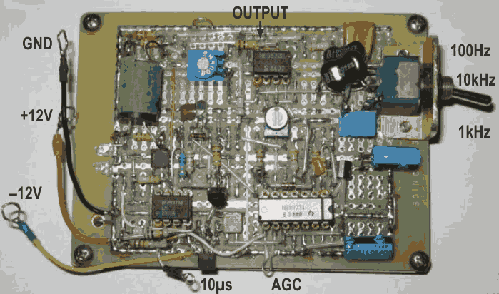
The photo in Figure 1 shows the prototype board, mounted on a sheet of blank copper-clad PCB material to provide shielding under the board. The optocoupler is the green cylinder at the top left of the board. Power, output, oscilloscope trigger (10 µs) and AGC outputs are shown, although your layout will no doubt be different from that pictured. There are no plans for a PCB at this stage, and it's unlikely that there will be enough interest to warrant the time and cost for design and production. The photo does give you some idea of how compact it can be, and the prototype measures just 95 × 70 mm. I expect it will be easier to build if you allow a bit more space.
 |
|
| Figure 1. | Photograph of Tom's prototype oscillator. |
Tom (it's designer) calls it a 'wicked fast, ultra low distortion oscillator', because the stabilisation system is very fast indeed. Rather than using a filter which can have a significant settling time, it uses a sample and hold (S/H) technique to monitor the AC output level. The S/H ensures that there is close to zero ripple on the hold capacitor, so the LDR used for amplitude stabilisation has no superimposed AC component which degrades the oscillator's distortion figure. By avoiding the conventional rectifier and filter, the oscillator can stabilise in only a few cycles. That definitely qualifies as 'wicked fast'.
The voltage across the LDR is kept as low as possible. Although LDRs are far more linear than JFETs, they do introduce some easily measurable distortion, which is worse when the voltage across the LDR is high. More voltage, more distortion, and vice versa.
In this design, the voltage across the LDR is maintained at less than 100 mV peak for a normal 3 V RMS output signal.
Circuit description
Tom worked out the sample and hold circuit in 1987 for John Linsley-Hood's 'Spot Frequency Distortion Meter'. It uses JLH's arrangement of the Wien-bridge (Wireless World, May 1981 [2]) and gets the same distortion as his did at 1 kHz (0.001%), but also at 100 Hz and it really is 'super wicked fast'.
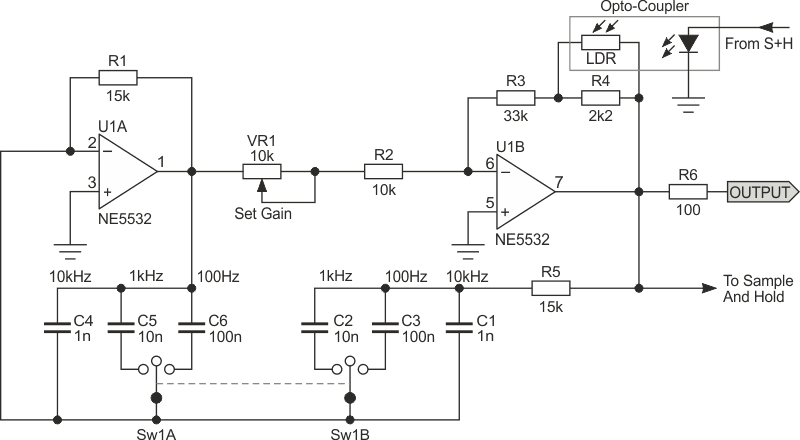
It also works down to 10 Hz with (much) larger capacitors. This is very difficult to achieve any other way, unless a very long filter time constant is used, and that means the oscillator will take several seconds (up to a minute or more at very low frequencies) to stabilise. The oscillator is shown Figure 2, and it's a Wien bridge design using two inverting opamp stages. This is done to eliminate opamp common mode distortion, which is produced (albeit in small amounts with good opamps) when there is a significant common mode voltage at the opamp inputs (i.e. a voltage applied to both inputs simultaneously with respect to ground).
 |
|
| Figure 2. | Oscillator schematic. |
It may seem that using two opamps is overkill for a Wien bridge oscillator, because most use just one (or a discrete version where high frequencies are needed). However, this arrangement is preferable for minimum distortion. The idea of using inverting opamps and an LDR to control the level is used in many circuits on the Net, but most (including the JLH design) employ a traditional rectifier and filter to minimise ripple through the opto-coupler's LED. This makes them slow to settle, and much more so if low frequencies are required. The original JLH circuit that was used as the basis for this circuit used a rectifier and filter arrangement (but used TL072 opamps rather than the NE5532 suggested here).
The oscillator is fairly conventional. As noted, it uses a Wien bridge to set the frequency, and is provided with a gain control to ensure reliable start-up. The gain needs to be set carefully, so there is just enough gain to ensure that oscillation starts every time. If the gain is too low, there will be no output at all. Once the circuit is oscillating, the gain is reduced by the LDR in the opto-coupler. It has a limited range, and it will be unable to control the level if the gain is too high.
Three frequencies are provided, nominally 100 Hz, 1 kHz and 10 kHz. The actual frequencies depend on the accuracy of the resistors and capacitors (R1 and R5, and C1 … C6). The theoretical frequencies (assuming exact values) are 105 Hz, 965 Hz and 10.6 kHz. Because Sw1 is a centre-off switch, the centre position is 10 kHz. You can use a rotary switch if preferred, so the frequencies will be in order (i.e. 100 Hz, 1 kHz and 10 kHz).
The gain of U2 is theoretically exactly two, assuming that all tuning values are exact. In reality, a gain of slightly more is necessary to allow the oscillator to start, and to account for tuning component tolerances. VR1 is used to adjust the gain so that the circuit oscillates at all three switch positions. Note that if the capacitors are not selected to within 2% or so, it may not be possible to set the gain such that the circuit oscillates reliably and has sufficient gain control range.
Sw1 is a 2-pole centre-off switch. When centred, the frequency is 10 kHz (C1 and C4), and the other caps are switched in parallel to obtain 100 Hz (C3 and C6) or 1 kHz (C2 and C5). Note that C4, C5 and C6 are in parallel with R1 (the parallel section of the Wien bridge) and C1, C2 and C3 are in series with R5 (the series section).
Tuning capacitors should be polystyrene for low values, and polypropylene (MKP) for the higher values. Although polyester (MKT) caps can be used, they will almost certainly degrade the distortion performance slightly. It's up to the constructor to decide whether the extra expense of MKP or polystyrene caps is warranted. The test oscillator that Tom sent me for evaluation appears to use some MKT caps, and the distortion remains below the limits I can measure (it's well below 0.01% THD).
References
- Sinewave Oscillators
- “Wien-bridge Oscillator With Low Harmonic Distortion“ - John Linsley-Hood (Wireless World, May 1981)
- DIY LED/LDR Optocoupler
- “Vannerson-Smith Low Distortion Oscillator“ - Eric Vannerson and K. C. Smith (University Of Toronto, 1975)