The sample and hold circuit (Figure 3) is considerably more complex than the oscillator. This is unfortunate but unavoidable. It's the S/H that gives this design its speed (fast settling time) and very low distortion, and it's very unlikely that a less complex but more 'conventional' rectifier and filter can achieve results that are anywhere near as good. While distortion may be equalled, settling time will be dramatically worse because of the long filter time constant needed for acceptable filtering.
 |
|
| Figure 3. | Sample & Hold Schematic. |
By way of contrast, the 1981 JLH design (1 kHz only) has a filter time constant of over 3 seconds to achieve the same distortion figure. It will typically take more than 1 second before it can provide enough feedback to limit the distortion to the claimed figure. The circuit is only marginally less complex than that shown, and it needs electrolytic capacitors in the filter section. If lower frequencies are needed, the settling time will be a great deal longer, because the filter needs even larger capacitors!
As the incoming sine wave rises to its peak, the cap (C9) on Pin-2 of the comparator (U3A) momentarily holds that peak (at a diode drop below peak). As the sine wave (relatively) slowly drops below the voltage across C9 (so the voltage on U3A-Pin-3 falls below U3A-Pin-2), the comparator 'snaps'. The output pulse is differentiated by C10, which produces a positive pulse of (nominally) 10 µs. The pulse turns on Q2, and the sample voltage held on C9 is transferred to the AGC hold capacitor (C11). This value is held for a considerable time, as there is no discharge path unless the JFET (Q2) is turned on.
The peak value across C9 is also held steady during the 10 µs sample time, as the sinewave transitions down to discharge the cap for another cycle. The extra drop across the LED (D3) allows the charge on C9 to hold for long enough to allow proper operation at all available frequencies. The hold-up time on C9 is about 100 µs with a 1 kHz output, and it varies with frequency. A sample is taken on each cycle of the input voltage (the output of the oscillator), ensuring that the sinewave amplitude remains constant.
The secondary comparator (U2B) detects if peak amplitude from the oscillator falls below around 120 mV (depending on the level setting used). If that occurs, it means the oscillator has stopped, so the hold capacitor is discharged to turn off the optocoupler and allow maximum gain so the oscillator will re-start. The most common reason for the oscillator to stop is when a transient is created as you switch frequency, and this charges the hold capacitor to a higher than normal voltage. The LDR then has minimum resistance, the oscillator gain is too low, so oscillation ceases. Note that the second half of U3 is not used. Feel free to use a quad opamp (TL074) rather than two dual opamps as shown in Figure 3, but one opamp is still unused. (Note that any unused opamp should have the +VE input grounded, and join the output and –VE input to prevent instability.)
As noted earlier, the AGC circuit for any sinewave oscillator is the real key to obtaining low distortion. Most competent opamps have extremely low distortion, even accounting for common mode voltages in a simple one-opamp Wien bridge circuit. If a 'perfect' electronically variable resistor were available, the gain stabilisation network would be easy. Figure 2 shows the complexity necessary to achieve a high performance circuit in the real world.
Waveforms
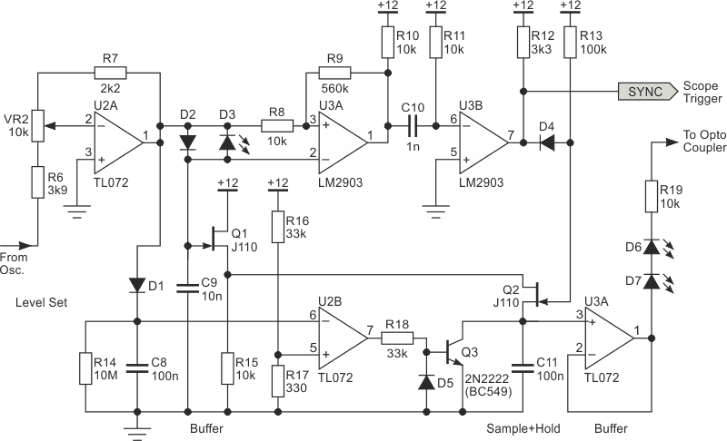
The sinewave itself is not the least bit interesting, because the distortion is so far below the resolution of the scope. The distortion residual is another matter, and it shows predominantly the fundamental, because my analyser can't null any further. There is some noise apparent, some of which is from the oscillator and some from the distortion meter itself. The sinewave and residual are shown below in Figure 4. Similar results were obtained from my other distortion meter, but it has a great deal more internal noise than the one used.
 |
|
| Figure 4. | Sinewave and distortion residual. |
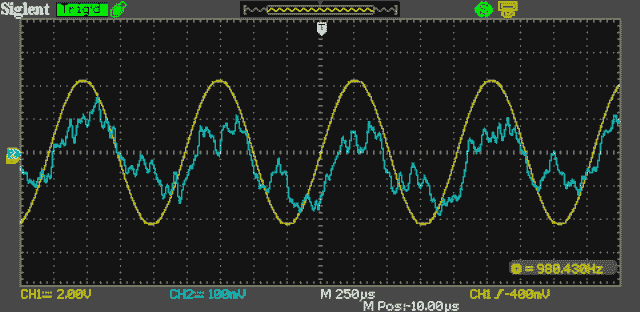
Next, the 10 µs S/H gating waveform is shown in Figure 5. It samples the positive peak, although it appears below to sample the negative peak of the output waveform because the input amplifier (U2A, which sets the output level) is inverting. This is of no consequence, because the waveform is perfectly symmetrical, as expected of a very low distortion sinewave. Subsequent tests with a more sensitive distortion meter revealed that the distortion is below 0.002%. How much below is difficult to judge, but the residual was predominantly noise. I'd estimate the true distortion to be no more than 0.001%, and probably less.
 |
|
| Figure 5. | Sample & hold gating waveform. |
If your board layout is imperfect, you may see a small residual of the gating pulse on the output waveform. Provided you keep the two sections separated, this will not affect the distortion because the level will be too low for it to have any effect. There's no evidence of it on the distortion residual shown in Figure 4, and the measurement was done using Tom's original layout with no additional shielding used.
Feel free to add a shield between the oscillator and the sample and hold circuits. This will minimise any high frequency noise passing from the S/H to the oscillator.
Notes
- The two LEDs in the AGC line compensate for DC across the 10k source in the FET buffer (Q1). They let the oscillator get going before the AGC kicks in.
- The oscillator can lock up during range switching and never run again. Droop on the hold capacitor is about 1 mV/sec, so if the oscillator stops with about 6 volts on the AGC line, that's about 6,000 seconds, or until you turn it off and on again. The additional rectifier and discharge transistor (Q3) at the bottom of the diagram takes care of that.
- The FET buffer is not an absolutely necessity either, but it does allow for a larger holding cap.
- Droop is not an issue, but some 'signal feedthrough' can degrade that ruler flat AGC line in this simple S/H. Making the holding cap (C11) large (brute force) swamps that out.
- Small 10 µs pulses appearing on the AGC line are due to 'gate charge transfer' in the sampling switch, but again this is not an issue because thankfully the LDR is too slow to see them.
- Worst case scenario is that fast spikes show up when observing THD residual on a 'scope. They are too narrow to contribute to an RMS value, but they are easy to reduce to an almost unobservable minimum with proper equipment grounding and supply bypass around the comparator.
- Scope sync is the output of either comparator for monitoring residual THD.
- RF radiation is not a problem, but some shielding from hum is necessary. It gets in on the high Z nodes like the hold buffer pin 3.
Optocoupler
You can make your own (as described in [3]), or you can use a commercially made unit. The Vactrol VTL5C4 or NSL-32SR3 would be ideal. The one used in the prototype is from an old Clairex CLM 3600, but another LED/LDR worked much the same. It has around 100 mV AC across the LDR. LDRs are non-linear with voltage, as are diodes, FETs and analogue multipliers.
It may be necessary to trial a few different LDRs to find one that has the lowest distortion. I've used LED/ LDR optocouplers in many designs over the years, and they are normally fairly linear if the voltage across them is kept low. It's quite easy to make your own if you have access to LDRs. Worst-case distortion on most 'simple' auto gain control elements (lamps and thermistors, but especially JFETs and LDRs) is when their internal resistance is reduced such that the signal level is reduced by 6 dB (half voltage).
Distortion is also directly related to the voltage across JFETs and LDRs. By keeping the voltage as low as possible, distortion is minimised.
References
- Sinewave Oscillators
- “Wien-bridge Oscillator With Low Harmonic Distortion“ - John Linsley-Hood (Wireless World, May 1981)
- DIY LED/LDR Optocoupler
- “Vannerson-Smith Low Distortion Oscillator“ - Eric Vannerson and K. C. Smith (University Of Toronto, 1975)