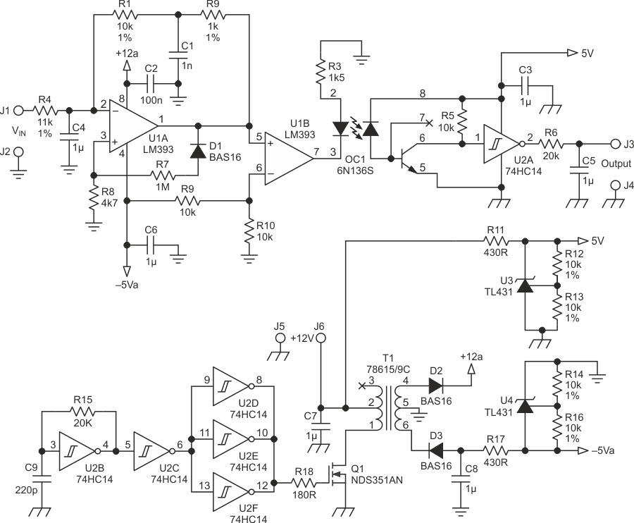
The isolation amplifier circuit of Figure 1 is simple but accurate. With the values shown it converts 0 to 5 V DC or low frequency signals with unity gain, but you can adjust the gain by changing R4.
 |
|
| Figure 1. | The floating sigma-delta converter U1 generates a pulse train whose duty cycle depends on the voltage at J1 and J2. The filtered DC level is reconstructed at the output J3. |
The lower half of Figure 1 is a DC to DC converter providing +12 V and –5 V to the isolated portion U1A and U1B. U2B through U2F is an oscillator and driver for Q1 which acts as a forward converter. The miniature transformer has been selected for its low interwinding capacitance, high primary inductance, and adequate leakage capacitance, which limits Q1's peak current. Because the frequency is high (about 300 kHz) and the primary inductance high (10 mH), the energy stored in the transformer is so low (15 mW avg.) that there is no need for snubber components, and Q1 itself clamps the overvoltage at turn off.
The isolation amplifier formed by comparator U1 works as a sigma-delta converter, with C4 as the integrating capacitor. The input voltage at J1 charges C4 through R4. When U1A's output goes low, C4 discharges to –5 V through R1 and R2. D1 and R7 introduce a small hysteresis. When C4's voltage is below the hysteresis value, U1A output switches to a high level (open), C4 recharges again thorough R4 and the cycle starts again. The output pulse duty cycle varies relative to the level at J1. Due to the negative feedback, the average pulsed output of U1A has to be the same as the input voltage since R1 + R2 = R4.
U1B buffers the output and drives the optocoupler LED on when the output of U1A is low at –5 V. U2A toggles following the same duty cycle pattern as U1, so the output average voltage filtered by R6 and C5 is the same as the average output of U1. The maximum linearity error is 1.3% from 5 V to 0.2 V. The switching frequency is about 3100 Hz at 4 V, 1360 Hz at 0.4 V, and goes down to 327 Hz at 90 mV. For increased accuracy at low input voltage, R2 and C1 mimic the delay in OC1, ensuring that the delays through the isolated and non-isolated parts are the same.
 |
|
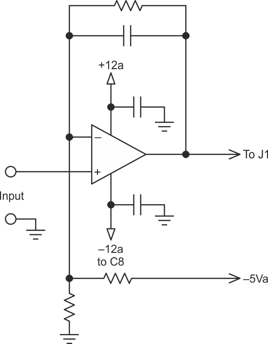
| Figure 2. | You can use a generic level shifter to offset negative input levels (relative to J2) to positive-only at J1. |
The circuit has been used in pH and Redox amplifiers, and to isolate the speed signal in three-phase AC inverters. If the input is both positive and negative relative to the isolated ground, you can use a circuit such as shown in Figure 2 to introduce a DC offset to U1A to always get a positive output.