On two days in the course of every year, one in March heralding the start of spring and another in September marking the first of fall, the Earth’s axis of rotation aligns perpendicular to the rays of the Sun. These days are the equinoxes and, as the name implies, divide daytime into nominally equal intervals of sunlight and night.
Author of multiple EDN design ideas, Jim McLucas (Mr. Equinox) evidently has a passion and a talent for devising circuits that also divide up time into equal intervals. He has published several clever and innovative design ideas that convert arbitrary waveshapes into 50:50 square waves, thus slicing and dicing the time axis into equal segments. He’s also often included a wide-range frequency doubler functions:
- Convert any signal to exactly 50% duty cycle (Ref. 1)
- Frequency doubler with 50 percent duty cycle (Ref. 2)
- Fast(er) frequency doubler with square wave output (Ref. 3)
I thought this looked like a fun concept and design challenge, and Jim kindly gave me permission to borrow it and try designing an “equinoctial” circuit of my own. Figure 1 shows the result.
Figure 1’s circuit comprises two almost identical sections: input processor, IP (U1pin1 through A1), and output generator, OG (U1p12 through A2).
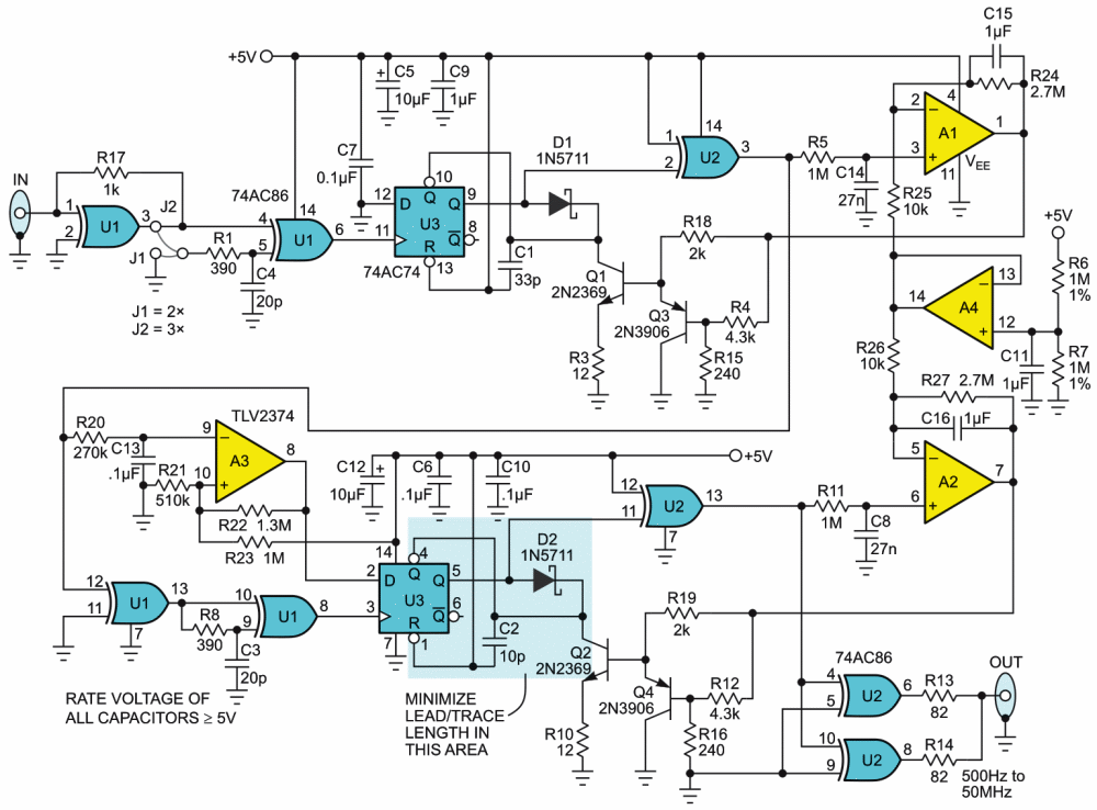 |
|
| Figure 1. | Kibitzer’s version of a McLucas frequency multiplier and square wave generator. |
The IP is capable of working in either of two modes as selected by jumper J1 or J2. J1 puts the IP into 50:50 mode in which it will accept any duty cycle input and convert it to a symmetrical 50% duty cycle square wave, suitable for frequency doubling by the OG. (This circuit concept is purely Mr. McLucas’s.) J2 puts the IP into frequency-doubling mode in which an input waveshape that’s already 50:50 symmetrical is doubled before input to the OG for net frequency quadrupling.
When frequency doubling J2 is selected, the combination of RC delays (R1C4 in the IP and R8C3 in the OG) and XOR gates (U1) generate high speed pulses (~6 ns width) on each input edge. Hence two pulses per cycle and doubled frequency input to the OG for quadrupled frequency. If J1 is jumpered instead, then R1C4 is bypassed and just one pulse per cycle and an unmultiplied 50:50 square wave is generated by the IP for doubling by the OG.
The hearts of both IP and OG are simple but fast timing loops in which a very fast monostable flip-flop is forced by feedback from an op-amp integrator to generate 50:50 square waves. (Yup. Jim’s idea again.)
My variation on Jim’s basic timing loop concept consists of U3’s two D type flip-flops and the surrounding components, including Schottky switching diodes D1 and D2, current sink transistors Q1 and Q2, and timing capacitors C1 and C2. Because the two loops are essentially identical, let’s talk about the OG loop.
Each timing sequence begins when U1pin8 delivers a clock pulse to U3 pin . U3 is positive-edge-triggered and responds by driving U3 pin 6 low. This disconnects D2 from timing cap C2 and allows the current sink Q2 to ramp it down toward the switching threshold of U3 pin 4 = –SET.
The timing interval thus begun has a duration (~10 ns to 500 µs) determined by Q2’s collector current as controlled in turn by integrator A2. The intent is to force the interval to be accurately 50% of the time between U1 pin 8 pulses. A2 does this by subtracting the 2.5 V reference developed by the R6R7 voltage divider from the pulse train at U2 pin 13 and accumulating the averaged difference on feedback capacitor C6.
If the duty cycle at U2pin13 is <50%, indicating that the U3 timeout is too long, A2’s output will ramp up, increasing Q2’s collector current and C2 ramp rate, thereby making the timeout shorter. If it’s >50%, A2 will ramp down, decreasing IC Q2 and lengthing the timeout.
Net result: after a few seconds, U2 pin 13 will output an accurately 50:50 square wave at 2 or 4 times (depending on J1 J2) the input frequency.
Provided, of course, that said frequency is within the limits of the timing loop.
The high end of said frequency range is mainly limited by the propagation delays of U3, Q2 ,and D2. These sum to about 10 ns (maybe a smidgeon less) and thus limit the max frequency to ~1/(10 ns + 10 ns) = ~1/20 ns = ~50 MHz (or possibly a bit more). The low end is limited by leakage currents (mainly through D2) that can cause C2 to continue to ramp down even when A2 turns Q2 completely off. This leakage can sum to upwards of 10 nA (especially if the diode is warm) and sets a bottom-end interval of ~1 ms and a temperature-dependent minimum frequency of (very) roughly ~1/(1 ms + 1 ms) = ~1/2 ms = ~500 Hz.
OG output is routed through U2 pins 6 and 8 and summed by R12 and R13 to produce a convenient 5 Vpp, ~50 Ω output. If no input is provided, the output shuts down at zero volts, preventing overheating of U2.
An additional detail is A3. It serves as an IP duty cycle comparator that holds OG timing loop activity disabled until the IP has converged (or nearly so) on and is producing an accurate 50:50 pulse train. This avoids the possibility of the erratic and persistent confusion of the OG feedback loop, which can occur if it’s allowed to try to converge prematurely.
It was indeed a fun project – all things being “equal”. Thanks, Jim!
References
- McLucas, Jim. “Convert any signal to exactly 50% duty cycle“.
- McLucas, Jim. “Frequency doubler with 50 percent duty cycle“.
- McLucas, Jim. “Fast(er) frequency doubler with square wave output“.