A while back, I published the Design Idea (DI) “Simple PWM interface can program regulators for VOUT < VSENSE” (Ref. 1)It showed some simple circuits for PWM programming of standard bucking-type regulator chips, both linear and switching, including applications that need an output voltage span that can swing well below the regulator’s sense voltage.
Recent reader comments have shown interest in applying those designs to different applications and regulators. So, here’s a step-by-step procedure to make that process easier.
Note that it only works if VX > 2VS and VL > VS.
 |
|
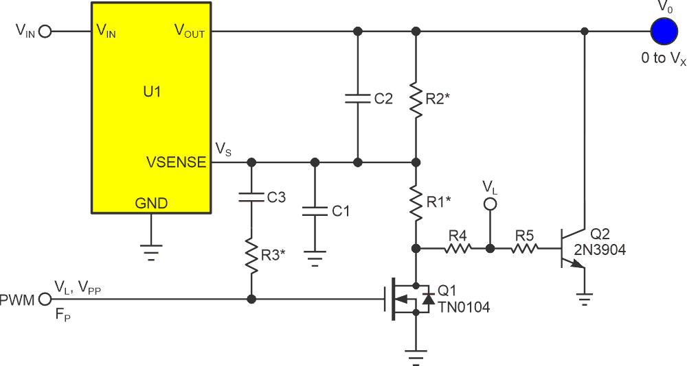
| Figure 1. | Ten discrete parts comprise a circuit for linear regulator programming with PWM. |
The steps are (Figure 1):
- VS = U1 sense voltage from U1 datasheet (typically 0.5 to 1.25 V)
- VL = available logic rail (typically 3 to 5 V)
- VX = desired maximum output voltage at PWM duty factor = 100%
- VPP = PWM peak to peak amplitude, typically VL
- FP = PWM rep rate
- N = PWM bits of resolution, N > 4
- R1 = recommended value from U1 datasheet example application
| 8. |  |
; |
| 9. |  |
; |
| 10. |  |
; |
11. R3 = Vpp/(Vs/R1 + (VL – VS)/(R1 + R4))
| 11. | 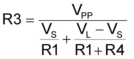 |
; |
| 12. |  |
; |
| 13. |  |
; |
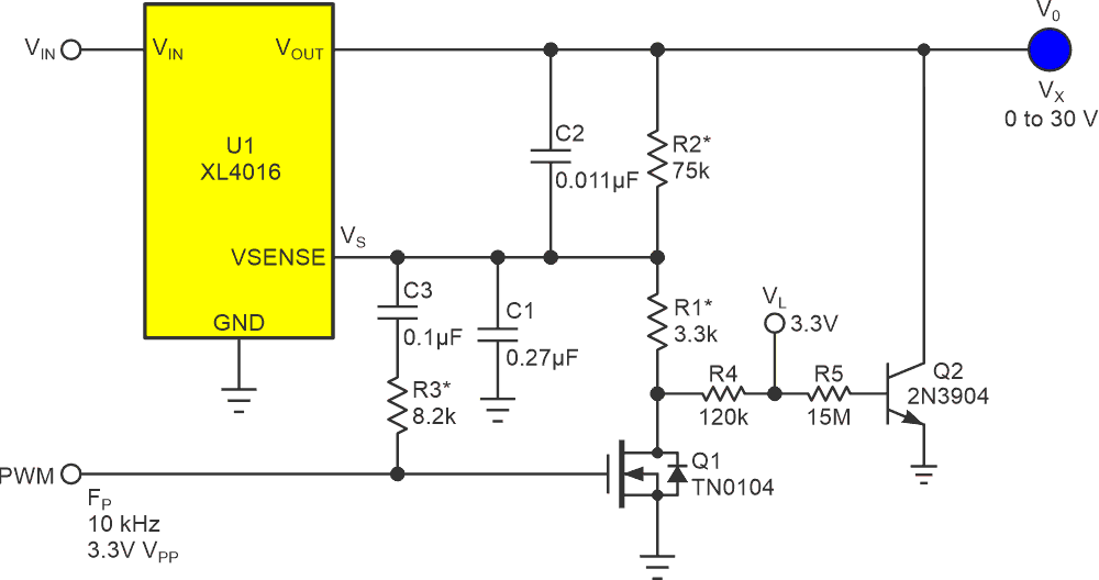
Now, taking the inexpensive XLsemi XL4016 asynch buck converter as an example case for U1, and turning the crank for these givens gives you:
- VS = 1.25 V
- VL = 3.3 V
- VX = 30 V
- VPP = 3.3 V
- FP = 10 kHz
- N = 8
- R1 = recommended value from U1 datasheet figure 4 = 3.3 kΩ
- R2 = 75 kΩ
- R4 = 120 kΩ
- R5 = 15 MΩ
- R3 = 8.2 kΩ
- C3 = 0.1 µF, C2 = 0.011 µF
- C1 = 0.27 µF
This yields Figure 2.
 |
|
| Figure 2. | General design-accommodating parameters listed above. Note that U1-specific parts (e.g., inductor, capacitors, and power diode) are not shown. |
Note that if the microamps and millivolts of residual zero offset that persist on the unloaded supply output at PWM = zero duty factor aren’t objectionable, then the Q2 R5 current sink is irrelevant and can be omitted.
Reference
- Woodward, Stephen. "Simple PWM interface can program regulators for VOUT < VSENSE."