My Design Idea (DI), “Flip ON Flop OFF for 48-VDC systems“ (Ref. 1), was published and referenced Stephen Woodward’s earlier “Flip ON Flop OFF” (Ref. 2) circuit. Other DIs published on this subject matter were for voltages less than 15 V, which is the voltage limit for CMOS ICs, while my DI was intended for higher DC voltages, typically 48 VDC. In this earlier DI, the ground line is switched, which means the input and output grounds are different. This is acceptable to many applications since the voltage is small and will not require earthing.
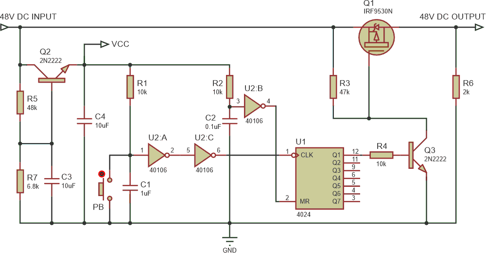
However, some readers in the comments section wanted a scheme to switch the high side, keeping the ground the same. To satisfy such a requirement, I modified the circuit as shown in Figure 1, where input and output grounds are kept the same and switching is done on the positive line side.
In this circuit, the voltage dividers R5 and R7 set the voltage at around 5 V at the emitter of Q2 (at VCC). This voltage is applied to ICs U1 and U2. A precise setting is not important, as these ICs can operate from 3 to 15 V. R2 and C2 are for the power ON reset of U1. R1 and C1 are for the push button (PB) switch debounce.
When you momentarily push PB once, the Q1-output of the U1 counter (not the Q1 FET) goes HIGH, saturating the Q3 transistor. Hence, the gate of Q1 (PMOSFET, IRF9530N, VDSS = –100 V, IDS = –14 A, RDS = 0.2 Ω) is pulled to ground. Q1 then conducts, and its output goes near 48 VDC.
Due to the 0.2-Ω RDS of Q1, there will be a small voltage drop depending on load current. When you push PB again, transistor Q3 turns OFF and Q1 stops conducting, and the voltage at the output becomes zero. Here, switching is done at the high side, and the ground is kept the same for the input and output sides.
If galvanic isolation is required (this may not always be the case), you may connect an ON/OFF mechanical switch prior to the input. In this topology, on-load switching is taken care of by the PB-operated circuit, and the ON/OFF switch switches zero current only, so it does not need to be bulky. You can select a switch that passes the required load current. While switching ON, first close the ON/OFF switch and then operate PB to connect. While switching OFF, first push PB to disconnect and operate the ON/OFF switch.
References
- Jayapal Ramalingam. "Flip ON Flop OFF for 48-VDC systems."
- Woodward, Stephen. "Flip ON Flop OFF."
