This versatile Design Idea survives and reports open- and short-circuits, not to mention multiplying efficiencies.
Generally accepted tech folklore says that after you drive relays and solenoids into full actuation, only half as much coil voltage and current – and therefore only a fourth as much power – is needed to hold them there. Consequently, driver designs that continuously apply full voltage burn four times the power and heat the coil four times hotter than the job
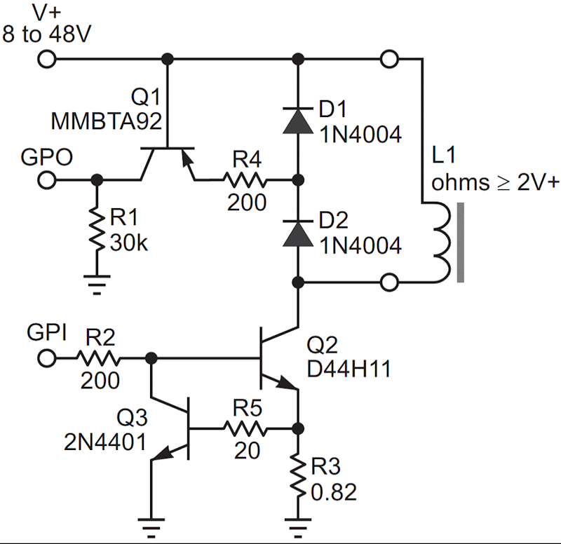
Figure 1’s driver circuit employs pulse width modulation (PWM) to dramatically diminish post-pull-in power waste. As an extra added bonus, it also survives and reports open- and short-circuit faults on the GPI status bit.
 |
|
| Figure 1. | In this circuit, driver transistor Q2’s PWM duty cycle varies from 100% at actuation to a power saving 50% sustain. It can accommodate load currents up to half an amp. R5 protects current limiter Q3’s base-emitter junction from destruction by over-current events. And Q1 detects coil opens and shorts. |
Here’s how it works.
The PWM signal on the general-purpose output (GPO) bit sets Q2’s conduction duty cycle from 0% to 100% to ~50%, from off to full voltage pull-in to quarter-power sustain. Q3 protects Q1 from over-current resulting from shorted coil faults. And Q1 utilizes relay/solenoid coil L1’s inductive “kickback” to detect correct driver operation and report it as a logic “1” on the general purpose input (GPI) pin… or, if kickback is absent (meaning the coil is open or shorted), its logical opposite, “0”.
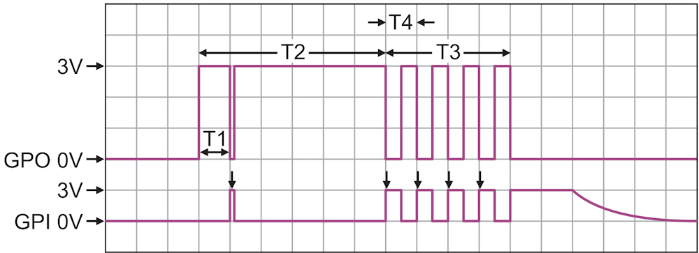
Figure 2 not-to-scale sketches the driver timing.
 |
|
| Figure 2. | In this timing diagram, T1 = timeout to first fault check = L1/R timeconstant = ~500 µs. T2 = ~100% PWM duty cycle to power initial actuation = ~10 ms. T3 = ~50% sustain duty cycle for as long as application requires. And T4 = PWM sustain cycle = ~100 µs = 10 kHz. |
In summary, Figure 1’s circuit neither squanders power nor requires changing component values to accommodate different supply voltages. And it’s simple. Along with, dare I say, beautiful? I guess I just did!