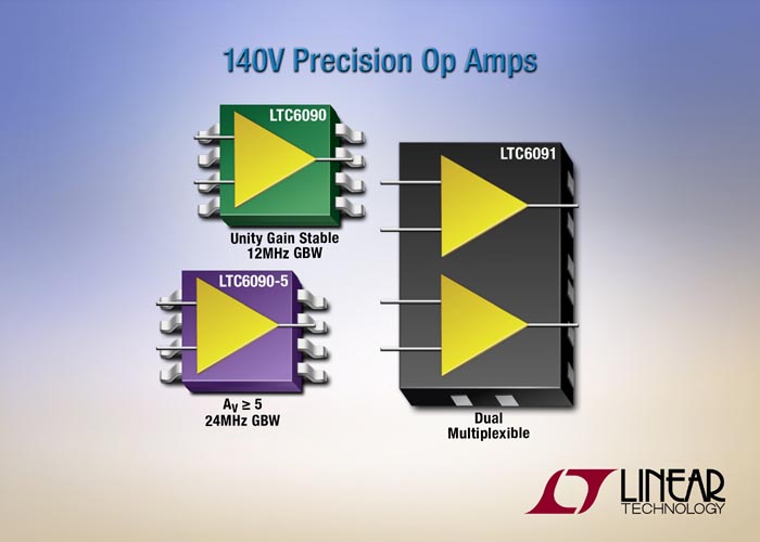
Linear Technology announces the LTC6091 and LTC6090-5, additions to the LTC6090 family of precision operational amplifiers which operate on a supply voltage up to 140 V (±70 V). The dual LTC6091 features separate output disable pins, making it useful in high voltage multiplexed applications. The decompensated single LTC6090-5 amplifier offers higher speed and is stable at a gain of 5 or above.

The LTC6090, LTC6090-5, and LTC6091 combine wide supply range, high precision, and low noise. Input offset voltage is 1.25 mV max over temperature, and low frequency (1/f) noise is 3.5 μV from 0.1 Hz to 10 Hz. The CMOS input structure keeps the input bias current to 50 pA maximum at 85 °C, making the LTC6090 family suitable for sensor circuits and other applications requiring high input impedance.
The decompensated LTC6090-5 offers 24 MHz gain-bandwidth product and 37 V/μs slew rate, compared with 12 MHz and 21 V/μs for the gain-of-1 stable LTC6090 and LTC6091.
Supply current is 3.9 mA per amplifier max. Output short-circuit current is typically ±90 mA. A thermal flag pin (TFLAG) signals when the device junction temperature exceeds 145 °C. This pin can be connected to the Output Disable pin for active thermal management.
The LTC6090 and LTC6090-1 are available in 8-pin SOIC and 16-pin TSSOP packages. The LTC6091 is offered in a 16-pin 4 mm × 6 mm QFN package. Each of these packages includes an exposed pad to minimize thermal resistance. Prices start at $3.45 each for the LTC6090 and LTC6090-5, and $6.61 each for the LTC6091 in quantities of 1,000.
The LTC6090 is available in three temperature range grades: 0 °C to 70 °C, –40 °C to 85 °C and –40 °C to 125 °C junction temperature. The LTC6091 is available in –40 °C to 85 °C and –40 °C to 125 °C junction temperature grades.
Summary of Features: LTC6091
- Supply Range: ±4.75 V to ±70 V (140 V)
- 0.1 Hz to 10 Hz Noise: 3.5 μV
- Input Bias Current: 50 pA Maximum
- Low Offset Voltage: 1.25 mV Maximum
- Low Offset Drift: ±5 μV/°C Maximum
- CMRR: 130 dB Minimum
- Rail-to-Rail Output Stage
- Output Sink & Source: 20 mA Minimum
- 12 MHz Gain Bandwidth Product
- 21 V/μs Slew Rate
- 11 nV/√Hz Noise Density
- Thermal Shutdown
- 4 mm × 6 mm 16-Lead QFN Package
Summary of Features: LTC6090-5
- Supply Range: ±4.75 V to ±70 V (140 V)
- 0.1 Hz to 10 Hz Noise: 3.5 μV
- Input Bias Current: 50 pA Maximum
- Low Offset Voltage: 1.25 mV Maximum
- Low Offset Drift: ±5 μV/°C Maximum
- CMRR: 130 dB Minimum
- Rail-to-Rail Output Stage
- Output Sink & Source: 50 mA Minimum
- 24 MHz Gain Bandwidth Product
- 37 V/μs Slew Rate
- 11 nV/√Hz Noise Density
- Thermal Shutdown
- Available in Thermally Enhanced SOIC-8E or TSSOP-16E Packages