Renesas Electronics introduced the industry’s first bidirectional switch using depletion-mode (d-mode) GaN technology, capable of blocking both positive and negative currents in a single device with DC blocking. Targeting single-stage solar microinverters, AI data centers and onboard electric vehicle chargers, the high-voltage TP65B110HRU dramatically simplifies power converter designs and replaces conventional back-to-back FET switches with a single low-loss, fast-switching, easy-to-drive device.

Single-stage topology boosts efficiency, reduces components
Today’s high-power conversion designs use unidirectional silicon or silicon carbide (SiC) switches, which block current in only one direction when in the off state. As a result, power conversion must be divided into stages with multiple switched bridge circuits. For example, a typical solar microinverter uses a four-switch full bridge to convert from DC to DC for the first stage, followed by a second stage to produce the final AC output to the grid. Even as the electronics industry moves toward more efficient single-stage converters, engineers must work around inherent switching limitations. Many of today’s single-stage designs use conventional unidirectional switches back-to-back, resulting in a four-fold increase in switch count and reduced efficiency.
Bidirectional GaN changes this landscape entirely. By integrating bidirectional blocking functionality on a single GaN product, power conversion can be achieved in a single stage using fewer switching devices. A typical solar microinverter, for example, will require only two high-voltage Renesas SuperGaN bidirectional devices, eliminating the intermediary DC-link capacitors and cutting the switch count by half. In addition, GaN products switch fast, with low stored charge, enabling higher switching frequencies and higher power density. In a real-world single-stage solar microinverter implementation, the new GaN architecture demonstrated higher than 97.5% power efficiency with the elimination of back-to-back connections and slow silicon switches.
Combining robust performance and reliability with silicon-compatible drivers
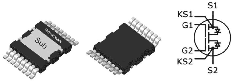
Renesas field-proven 650 V SuperGaN devices are based on a proprietary normally-off technology that is simple to drive and highly robust. The TP65B110HRU combines a high-voltage bidirectional d-mode GaN chip co-packaged with two low-voltage silicon MOSFETs with high threshold voltage (3 V) high gate margin (±20 V) and built-in body diodes for efficient reverse conduction. Compared with enhancement mode (e-mode) bidirectional GaN devices, the Renesas bidirectional GaN switch offers compatibility with standard gate drivers that require no negative gate bias. This translates to a simpler, lower-cost gate loop design and fast, stable switching in both soft and hard switching operation without a performance penalty. Power conversion topologies that require hard switching, such as the Vienna-style rectifier, can benefit from its high dv/dt capability of >100 V/ns, with minimum ringing and short delays during on/off transitions. The Renesas GaN device enables true bidirectional switching with high robustness, high performance and ease of use.
Key features of the TP65B110HRU
- ±650 V continuous peak AC and DC rating, ±800 V transient rating
- 2 kV Human Body Model ESD protection rating (HBM and CDM)
- 110 mΩ typical RSS,ON @ 25 °C
- 3 V typical VGS(th)
- No negative drive required
- ±20 V maximum VGS
- >100 V/ns dv/dt immunity
- 1.8 V, VSS,FW freewheeling diode voltage-drop
- TOLT top-side cooled package with industry standard pin-out
Availability
The TP65B110HRU bi-directional GaN switch is available in quantity today. Customers can also purchase the RTDACHB0000RS-MS-1 evaluation kit for testing with different drive options, detect AC zero crossings and implement ZVS soft switching.
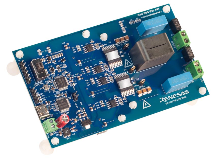 |
| GaN bidirectional switch half-bridge evaluation kit RTDACHB0000RS-MF-1-KIT. |