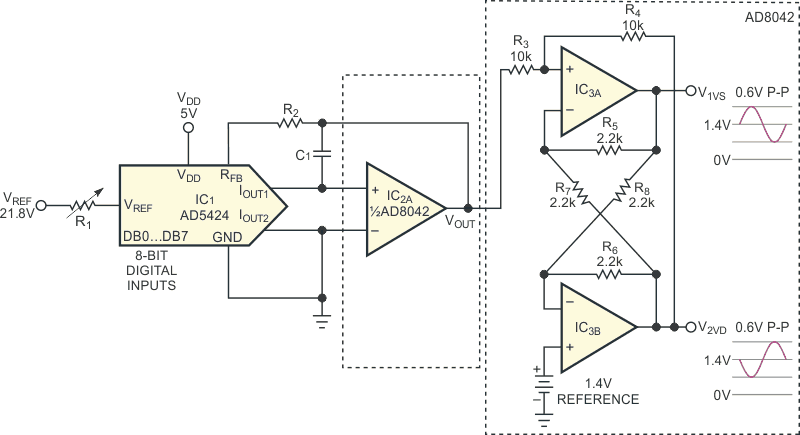
High-speed DACs offer differential outputs, but, for low-end ac applications or high-precision level-setting applications, a single-ended current-output DAC with a differential-conversion circuit provides a novel approach to generating differential-waveform-control functions. The basic circuit in Figure 1 combines a current-output DAC, IC1, such as the 8-bit AD5424 DAC, with a single-ended-to-differential op-amp stage – IC2, IC3A, and IC3B – to generate the desired outputs. For dual-power-supply applications, you select the DAC's unipolar mode of operation to achieve optimum performance from the DAC. Using a single op amp, the DAC provides two-quadrant multiplication or a unipolar output-voltage swing. The DAC's output requires a buffer because changing the code applied to the DAC's input varies its output impedance.
 |
|
| Figure 1. | This basic circuit combines a current-output DAC, IC1, with a single-ended-to-differential op-amp stage – IC2, IC3A, and IC3B – to generate the desired outputs. |
This equation defines the circuit's output voltage:
where N defines the number of input bits, VREF is the reference voltage, and D is the decimal equivalent of the binary code. To generate a positive common-mode voltage, you use a negative voltage for the DAC's reference voltage. The DAC's internal design accommodates ac reference input signals of –10 to +10 V. In this mode, the DAC provides a 5M-sample/sec maximum update rate for one-quarter full-scale code changes when you operate it from a 5 V power supply. Use resistors R1 and R2 only if your application requires adjustable gain.
The single-ended-to-differential stage comprises two cross-coupled op amps, which resistors R5 and R6 configure as a unity-gain follower. To yield a symmetric circuit, the outputs also drive each other as unity-gain inverters through R7 and R8. The voltage you apply to the positive terminal of op amp IC2 sets the circuit's common-mode voltage. Resistors R3 and R4 control the amplitude of the differential voltage. Review your application's output-load requirements and the op amps' input- and output-voltage capabilities.
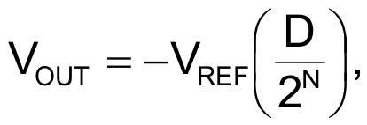
For single-supply applications, you can use a current-output DAC in reverse mode, in which you apply the reference voltage, VIN, to the DAC's IOUT1 pin and take the output voltage from the DAC's VREF terminal (Figure 2). In this configuration, a positive reference voltage produces a positive output voltage. This circuit does not use the DAC's feedback resistor, RFB, and its connection to IOUT1 prevents stray capacitance effects. The DAC's reference input “sees” an impedance that varies with the applied code and thus requires a low-impedance source.
Note that the switches in the DAC ladder no longer have the same source-to-drain drive voltage, which in turn limits the input voltage to low voltages. As a result, the switches' on-resistances differ and degrade the DAC's linearity. Also, this mode limits the maximum update rate to 1.5M samples/sec. You can use sections of a dual op amp to buffer the DAC's input and to amplify the DAC's output voltage (Figure 3). The circuit's intended application determines your choice of supporting amplifiers. For lower speed, precision applications, the op amp requires low input-bias currents and low input-offset voltage to avoid degradation of the DAC's DNL (differential-nonlinearity) performance. For example, the AD8628 offers 100-pA maximum bias current at room temperature and 5-µV maximum input-offset voltage. The op amp's low-frequency noise is important in precision level-setting applications, and the AD8628 specifies 0.1- to 10-Hz noise of less than 0.5 µV p-p. Its rail-to-rail inputs and outputs make it ideal for use in single-supply circuits.
For high-speed-system applications, the op amp's slew rate must not dominate the DAC's slew rate. The op amp's bandwidth must be large enough to drive the feedback load and must not limit the circuit's overall bandwidth, and the DAC's output- voltage settling time should determine the circuit's maximum update rate. The AD8042 in figure 1 and figure 2 offers 170-MHz bandwidth and a 225 V/µsec slew rate, allowing it to easily achieve these results. Other high-speed op amps, such as the AD8022, AD8023, and AD8066, also work well in this application.
 |
|
| Figure 2. | In this configuration, a positive reference voltage produces a positive output voltage. |
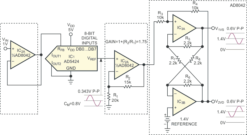
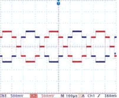
The DAC consumes only 0.4 µA of power-supply current, and the op amps thus dominate the circuit's power consumption. To minimize the area for the circuit on a pc board, you can replace all four op amps in Figure 2 with a single AD8044 quad op amp. The single-ended-to-differential conversion of a digitized, eight-point sine wave in the presence of a 1.4 V common-mode voltage and a 0.6 V differential signal produces differential outputs (Figure 3).
 |
|
| Figure 3. | The single-ended-to-differential conversion of a digitized, eight-point sine wave produces differential outputs. |