Because of process limitations, all ICs have an input-voltage limitation. This limitation can be cumbersome when you try to step down a high supply voltage to a lower, regulated voltage using a dc/dc converter, such as a linear regulator. Adding a FET to the input of a linear regulator creates a dc/dc converter with a wider input-voltage range than the range of the regulator alone. The excess voltage and, therefore, power occurs in the FET.
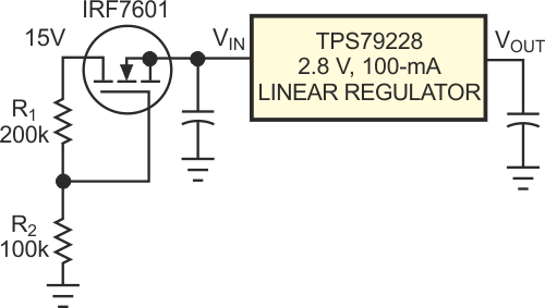
Figure 1 shows an IRF7601 n-channel MOSFET on the input of a TPS79228 2.8 V, 100-mA, low-noise, high-power-supply rejection ratio low-dropout regulator. R1 and R2 provide a bias voltage to the gate of the MOSFET, and the load current determines the voltage at the source of the MOSFET. (In other words, the FET's on-resistance adjusts to accommodate the load current.) In this example, the maximum power-supply voltage is 15 V, but the TPS79228 has a maximum recommended operating input voltage of 5.5 V, so this design uses a MOSFET with a 20 V breakdown voltage.
 |
||
| Figure 1. | You can use a MOSFET switch to expand a low-dropout regulator’s input-voltage range. |
|
To determine the minimum bias voltage for the gate of the MOSFET, you need the MOSFET's drain-current, ID,-versus-gate-source voltage, VGS, data-sheet curves. For the IRF7601, the curves indicate that the device needs VGS slightly below 1.5 V for 100-mA output current. Because the maximum dropout voltage of the regulator is 100 mV at 100 mA, the regulator's input voltage must stay above 2.9 V. Therefore, you must bias the gate of the MOSFET to at least 1.5 V+2.9 V = 4.4 V. Thus, when the MOSFET provides 100 mA, its source voltage does not drop below 2.9 V. The maximum gate-bias voltage is simply the maximum recommended operating voltage for the regulator, or 5.5 V. This voltage provides more than enough gate drive to provide the regulator's 1 µA of quiescent current during shutdown mode. Although you can bias the gate between 4.4 and 5.5 V, this design uses a bias voltage of 5 V to account for variations in the threshold voltage. Maximum power dissipation for the FET is
100 mA × (15 V – 2.9 V) = 1.21 W.
The IRF7601, in a Micro 8 package, can handle this power figure at an ambient temperature of 55 °C.
 |
||
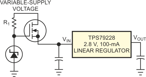
| Figure 2. | A zener diode provides fixed gate drive to the MOSFET when the input voltage varies significantly. |
|
The circuit in Figure 2 is slightly more complicated but may be necessary if the input voltage varies significantly. A zener diode replaces the R2 in Figure 1 and provides a fixed gate drive to the MOSFET. You select the output voltage of the zener diode in a manner similar to that explained above. Either of the two methods is acceptable for creating a dc/dc converter with a wider input-voltage range than the converter IC allows. The single-MOSFET solution is the simplest and least expensive solution. The MOSFET biased with a zener diode is the best choice when the supply is unregulated.