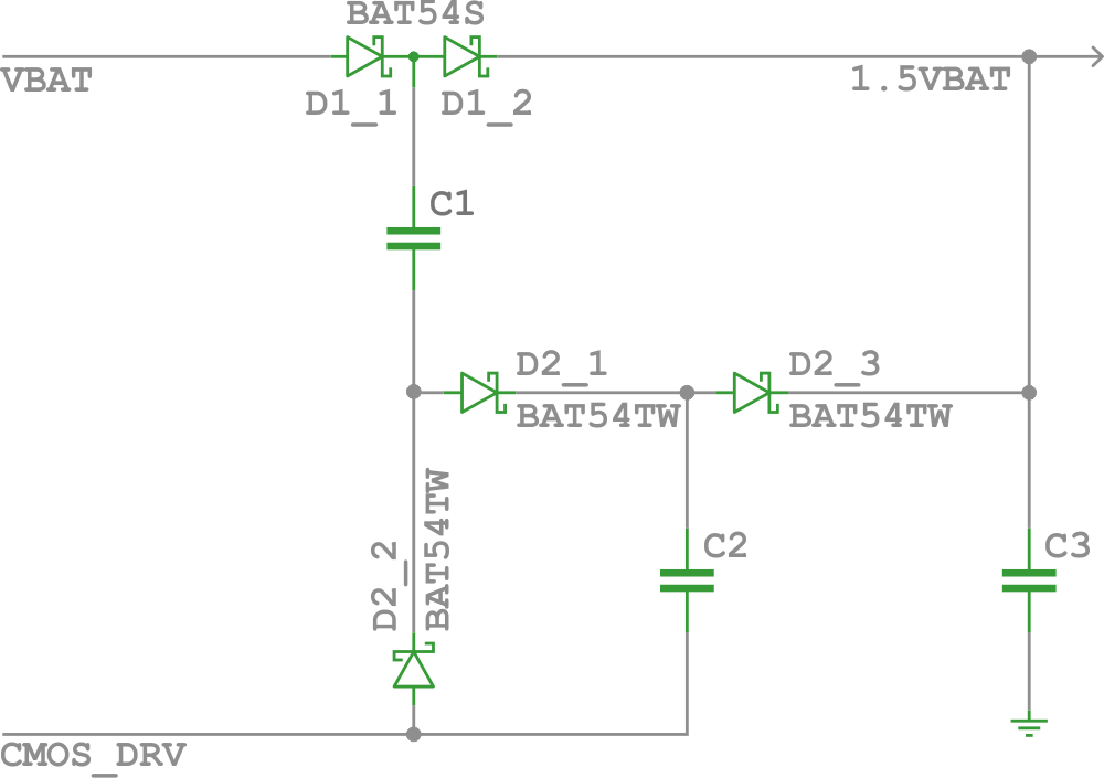
This charge-pump circuit, using just a few diodes and capacitors, ups the input voltage by a factor of 1.5 in contrast to the usual voltage-doubling output.
Micropower product designs sometimes require a simple, inexpensive voltage booster to augment the system battery voltage, and that job often falls to a simple voltage-doubling charge pump. However, as seen from the battery side, the resultant doubling of the boosted-voltage load’s current is a heavy penalty to pay in cases where voltage doubling produces a higher voltage than is required. In such cases, a 1.5X voltage booster may be more appropriate (see Figure 1).
 |
||
| Figure 1. | A simple, switched charge-boost arrangement of diodes and capacitors produces an output that’s 1.5 times the input-rail voltage. |
|
The booster is driven by a CMOS IC’s output. When that output is low, C1 and C2 are in series and charged through D1-1 and D2-1. When the output is high, they’re in parallel with C1 discharging into C3 via D1-2 and D2-2 and C2 discharging into C3 via D2-3. (C1 and C2 share current, as during each discharge cycle they are essentially connected in parallel, to within one diode-voltage drop.) As expected, load current on the boosted side, seen on the input side, is multiplied by a factor of 1.5.
Schottky diodes are preferred to conventional diodes due to their much-lower voltage drop, which results in improved efficiency. The three capacitors can be the same size, with their value dependent on load current, maximum acceptable output-voltage ripple, and drive frequency. And the clock rate is a function of the first two of those factors along with capacitor value. Given the wide span of available capacitor values and clock rates, there’s considerable flexibility in their selection.
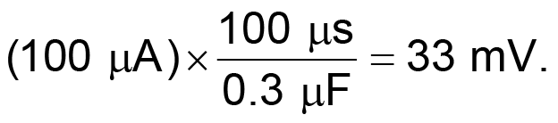
For example, assume a 5-kHz clock, and the requirement is to deliver 100 µA to the load with 133-mV maximum ripple. At that clock rate, the time to discharge C3 is about 200 µs (ignoring the short charge-transfer pulse every 200 µs). The first-cycle discharge (100 µs) occurs after charge transfer from C1 and C2 (and in parallel with C1 and C2), and the second-cycle discharge (also 100 µs) is C3 by itself. During the second cycle, C3 is discharged by the load current while C1 and C2 are charging. Standalone C3 discharge accounts for about three-quarters of the ripple voltage. Thus, for 100-mV ripple:
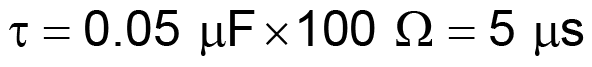
During the first cycle, charge is transferred from VCC to C1 and C2 in a pulse that’s much shorter than the discharge time of C3. Assuming drive-circuit output resistance ROUT of 100 Ω and identical capacitor values (C1 and C2 in series × ROUT drive), then charging-time equals
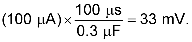
(which is much shorter than the C3 discharge time). During the first cycle, one-quarter of the ripple voltage occurs after charge transfer into C3 from C1 and C2. The ripple is due to the parallel discharge of the three capacitors. Since the load current is 100 µA while the parallel capacitance is 0.3 µF, the ripple voltage is
Thus, total ripple over the first and second cycles = 133 µV.