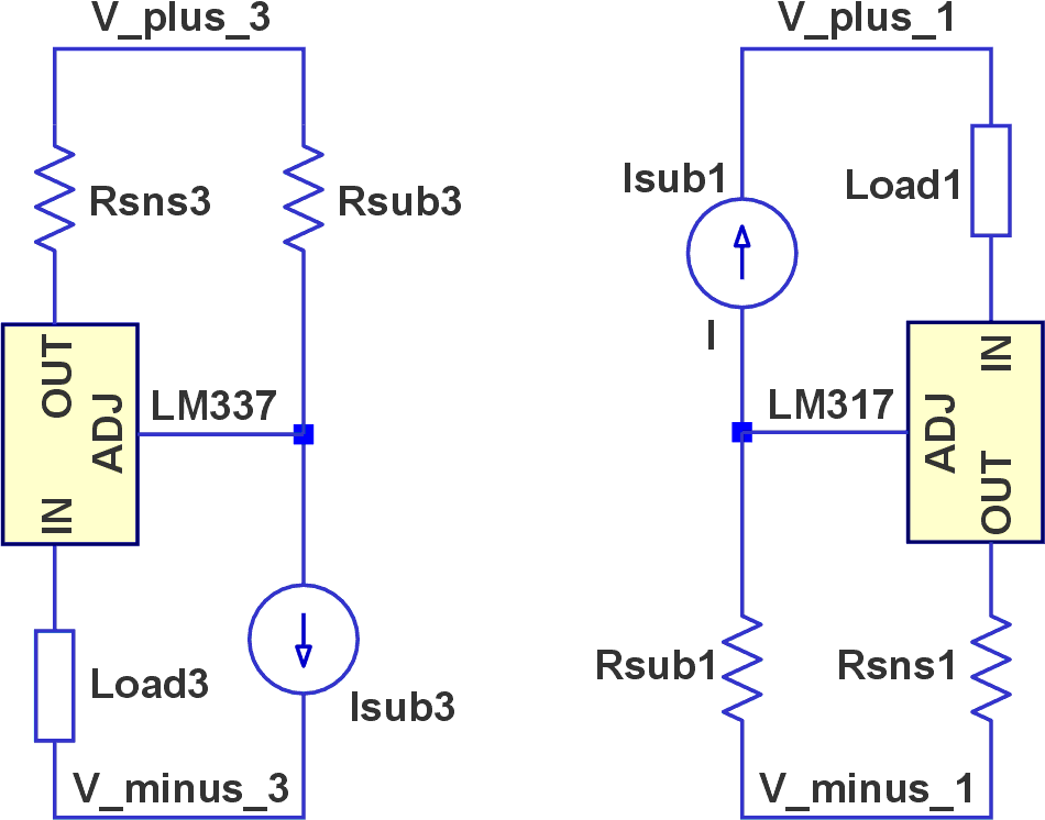
Several Design Ideas (DIs) have employed the subject ICs to implement programmable current sources in an innovative manner (References 1-3). Figure 1 shows the idea.
 |
|
| Figure 1. | Two independent current sources, one for loads referenced to the more negative voltage, and the other for those to the more positive one. The ISUB current sources control the magnitudes of the currents delivered to the loads. |
Each of the ICs works by enforcing VREF = 1.25 V (±50 mV over load current, supply voltage, and operating temperature) between the OUT and ADJ terminals. The ISUBs are programmable current sources (PWM-implemented or otherwise) which produce voltage drops VSUBs across the RSUBs.
Given that there are ADJ terminal currents IADJ (typically 50 µA and maxing out at 100 µA), the load currents can be seen to be:
When ISUB is 0, the load current is at its maximum, IMAX, and its uncertainty is a mere ±50 mV/1250 mV = ±4%. But when ISUB rises to yield a desired current of IMAX/10, the uncertainty rises to ±40%; the intended fraction of 1.25 V is subtracted, but the unknown portion of the ±50 mV remains. If IMAX/25 is desired, the actual load current could be anywhere from 0 to twice that value. Things are actually slightly worse, since the uncertainty in IADJ is a not-insignificant portion of the typically few-milliamp maximum value of ISUB.
Circumnavigating the accuracy limitations of reference voltages
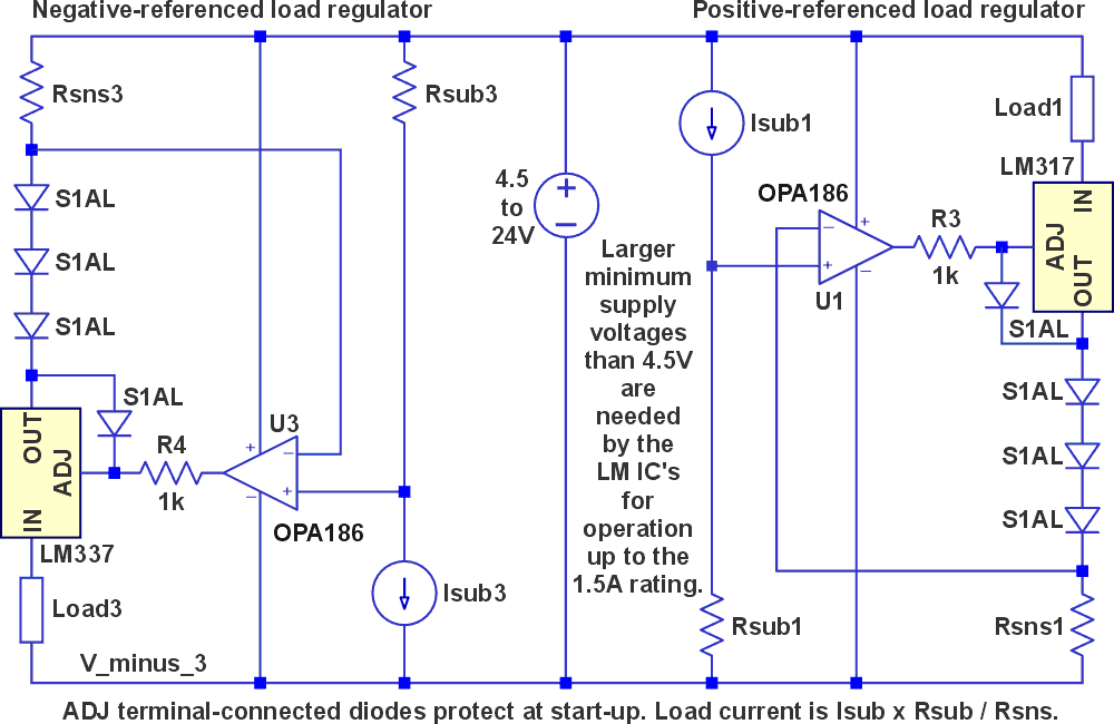
Despite the modest accuracy of their reference voltages, these ICs have the advantage of built-in over-temperature limiting. So it’s desirable to find a way around their accuracy limitations. Figure 2 shows just such a method.
 |
|
| Figure 2. | Two independent current regulators. The ISUB magnitudes are programmable and are often implemented with PWMs. Diodes connected to the ADJ terminals protect the LM ICs during startup. The 0.1-µF supply decoupling capacitors for U1 and U3 are not shown. |
The idea of the three-diode string was borrowed from the referenced DIs [Editor’s note: in “Related Content” below]. It ensures that even for the lowest load currents (the LM ICs’ minimum operating is spec’d at 10 mA max.), the ADJ terminal voltages needn’t be beyond the supply rails.
The OPA186 op-amp’s input operating range extends beyond both supply rails (a maximum of 24 V between them is recommended), and its outputs swing to within 120 mV of the rails for loads of less than 1 mA.
The maximum input offset voltage, including temperature drift and supply voltage variations, is less than ±20 µV. An input current of less than ±5 nA maximum means that for RSUBs of 1 kΩ or less, the total input offset voltage is 2000 times better than the LMs’ ±50 mV.
Placing the LM ICs in this op-amp’s feedback loop improves output current accuracy by a similar factor (but see addendum).
Adapting Jim Williams’ design for a current regulator
Jim Williams of analog design fame published an application note (Ref. 4) placing the LM317 in an LT1001-based feedback loop to produce a voltage regulator. Nothing prevents the adaptation of this idea to a current regulator. The LT1001’s typical gain-bandwidth (GBW) product is 800 kHz, almost exactly the 750 kHz of the OPA186, so no stability problems are expected. And there were none when the LM317 circuit was bench-tested with an LM358 op amp (GBW typically 700 kHz), which I had handy.
Just as you would with the Figure 1 designs, make sure the LM ICs are heatsinked for intended operation. Enclosing them in a feedback loop won’t help if their over-temperature circuitry kicks in. But under the temperature limit, this circuit increases not only load current accuracy, but also the IN-terminal impedances and the rejection of both the power supply and the LM’s references’ noises.
Note that some of the reduction in reference voltage error can be traded off to reduce power dissipation by making the RSNS resistors small. You can also convert the design to a precision voltage regulator by replacing the three-diode strings with a resistor and moving the load to between the OUT terminal and its RSNS resistor’s supply terminal.
Addendum
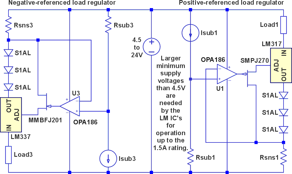
There’s a missing term in the equation given for load current. In Figure 2, the unknown and unaccounted-for amount of ADJ terminal current is added to the load current.
Considering that the LMs’ minimum specified operating current (see the LM317 3-Pin Adjustable Regulator datasheet and LMx37 3-Terminal Adjustable Regulators datasheet) – and therefore the minimum current through the load – is 10 mA at 25 °C, the ADJ maximum of 100 µA is small potatoes. Still, there might be applications where it would be desirable to account for it. Figure 3 is a possible solution, although I’ve not bench-tested it.
 |
|
| Figure 3. | Replacing the ADJ terminal-connected diodes with JFETs preserves startup protection for the LM ICs. |
The ‘201 and ‘270 JFETS route the ADJ terminal current through the RSNS resistors where it can be recognized and accounted for as part of the current that passes through the load. Cheaper bipolar transistors (which would reroute almost all IADJ) could be used in place of the JFETS, but that would require an additional diode in series with the three-diode string.
References
- Woodward, Stephen. "Cross connect complementary current sources to reduce self-heating error."
- Woodward, Stephen. "A negative current source with PWM input and LM337 output."
- Woodward, Stephen. "PWM-programmed LM317 constant current source."
- AN2 - Performance Enhancement Techniques for Three-Terminal Regulators