Lively discussions have sprung up here in editor Aalyia Shaukat’s Design Ideas regarding the limitations and quirks of, and design tricks for, the current control topologies shown in Figure 1.
 |
|
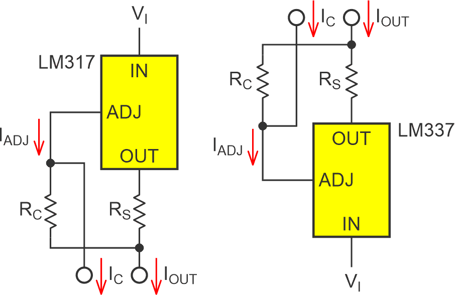
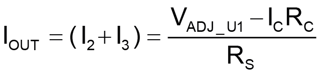
| Figure 1. | How to control amps of IOUT with mA of IC using legacy voltage regulators as current regulators where IOUT = (VADJ – ICRC)/RS. |
Reader Ashutosh Sapre contributed a disturbing observation about the likely effect on regulator reference accuracy of temperature rise from self-heating, as illustrated in Figure 2.
 |
|
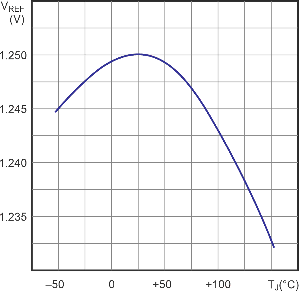
| Figure 2. | LM317 reference variation with junction temperature as seen in page 5 of LM317 datasheet. |
As shown in Figure 2, the temperature stability of these legacy devices is fairly good. Nevertheless, there are situations where the tempco can be problematic.
For example, consider a scenario that begins with programming for 100% of full-scale output current (e.g., 1 A) so that regulator heat dissipation is high. Assume it’s maintained long enough for the regulator’s junction temperature to rise from 25 °C to 125 °C. Figure 2 predicts that this large temperature swing will cause VREF to drift from 1.25 V to 1.2375 V, causing the output current to decline by about 1% of full scale.
This 1% corresponds to 10 mA out of 1000 mA and is somewhat less than 3 LSB of an 8-bit setting. That’s perhaps not great, but it’s not horrible either. But what if the output is then reprogrammed for 10% of full scale (e.g., 100 mA) while the regulator is still hot?
Then that 1% of full-scale error would become 10% of setting is what. It will manifest as a very lengthy thermal settling tail lasting many seconds as junction temperature gradually cools from 125 °C, allowing VREF to (slowly) return to its initial 1.25 V and output current to settle at the correct 100 mA. It will happen eventually, but the time required will be objectionable. It may be unacceptable.
Fortunately, Ashutosh also contributed a simple and practical solution to the problem in the form of an auxiliary current shunt transistor. The shunt would allow most of the output current and, consequently, most of the self-heating to bypass the regulator entirely. This would leave its junction unheated and its VREF undrifted. Problem solved!
Or is it? Ashutosh also pointed out that the bypass transistor, while handily solving the thermal problem, would unfortunately also bypass other things. Specifically, the nifty fault protection features (e.g., automatic current limiting and overheating shutdown) built into LM317 and LM337 chips would be lost. While these assets could potentially be added to the transistor shunt, that would lose much of the simplicity that made it attractive in the first place.
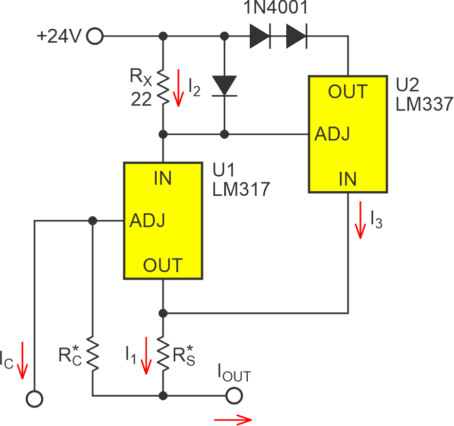
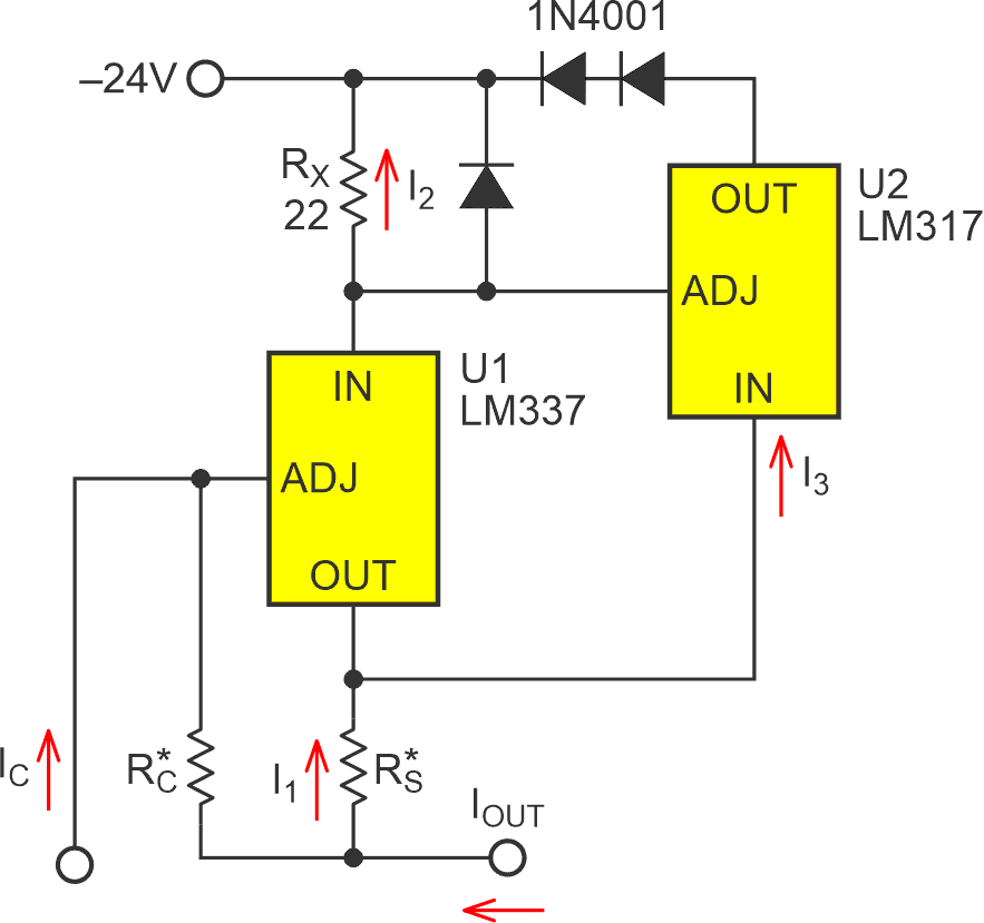
So, I wondered if Ashutosh’s shunt idea could be implemented in a way that would inherently retain the desirable 317/337 features while staying simple. The obvious thing (I like obvious!) might be to just make the shunt out of another LM3xx. Figure 3 shows just that: A design that cross-connects complementary regulators using U1’s 317 for control and U2’s 337 for shunt. Control and shunt currents are then summed back together before passing through RS to provide feedback to U1 where
and I3 >> I2. Notice how the shunt gets turned “upside down.”
Figure 3’s U1 is connected mostly per Figure 1, except for RX. The signal developed by RX × I2 feeds U2’s ADJ pin so that when U1 input current I2 rises above about 10 mA, U2’s ADJ pin will drop enough to make it start conducting. This causes the I3 current component to rise and ultimately comprise the majority of total current I1 = I2 + I3. Thus, U2 dissipates most of the self-heating Watts, ensuring that U1 remains relatively cool and its VREF remains accurate.
 |
|
| Figure 3. | Cross connection reduces self-heating error because shunt regulator U2 carries most of the current, getting relatively hot, while U1, whose VREF is in control, stays relatively cool and accurate. |
The 1N4001 in parallel with RX protects RX and U2’s ADJ pin if U2’s over-temp or over-current shutdown feature kicks in. That would leave U1 trying to shoulder the whole load, dropping enough voltage across RX to likely damage U2 and fry the resistor. The diode prevents that.
Figure 4 shows the idea working as a negative current source.
 |
|
| Figure 4. | If the 317 and 337 swap places and the diodes reverse, Figure 3’s circuit can work for negative current, too. |
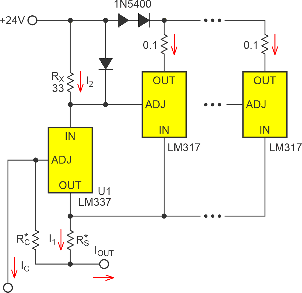
If more current capability is needed, more U2 shunts and higher capacity diodes can be added (Figure 5).
 |
|
| Figure 5. | Boost current handling capacity with beefier diodes and more U2s. |
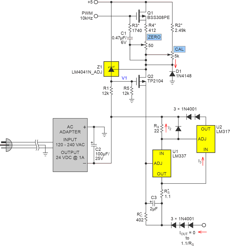
Figure 6 integrates this idea into a complete PWM controlled negative current source as detailed in: “A negative current source with PWM input and LM337 output” (Ref. 1)
 |
|
| Figure 6. | Negative current source circuit incorporates means for compensating component tolerances, including those of U1 and Z1 references. Note RS = 1.1 Ω and should be rated for more than 1 W. |
The one-pass adjustment sequence is:
- Set D = 100%
- Adjust CAL pot for 1 amp output current
- Set D = 0%
- Adjust ZERO pot for zero output current.
Done. IOUT = 1.1·D/RS, where D = PWM duty factor.
Reference
- Woodward, Stephen. "A negative current source with PWM input and LM337 output."