Any semiconductor has limits on how much voltage, how much current, and for how much time combinations of voltage and current can be supported in normal usage. Sometimes that information is provided as part of the device’s datasheet, and sometimes that information is NOT provided. In either case, though, there ARE limits which MUST be observed.
Any switching semiconductor device must address voltage and current issues. Drive considerations aside, from the standpoint of “safe operating area” or SOA, the voltage VDS and the current IDS of a power MOSFET and the VCE and IC of a bipolar transistor are at issue.
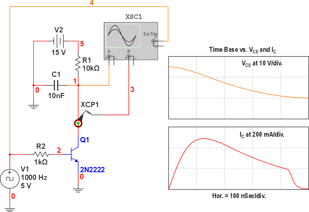
Please consider the following unwisely designed circuit in Figure 1.
 |
|
| Figure 1. | A badly designed switching circuit requiring the 2N2222 at Q1 to repeatedly dump the charge of capacitor C1 of 0.01 µF. |
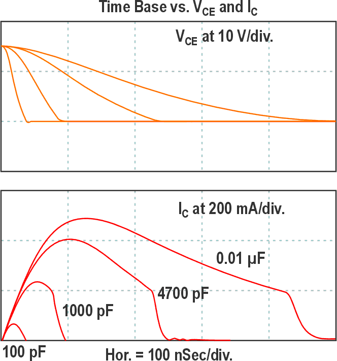
What we’ve done wrong here is require the 2N2222 at Q1 to repeatedly dump the charge of capacitor C1 of 0.01 µF. The VCE and the IC versus time burdens on Q1 are as shown. The current peak of nearly 500 mA is pretty big, and to our dismay, it occurs while the value of VCE is still fairly high, which means that there is a substantial peak power dissipation demand placed on Q1.
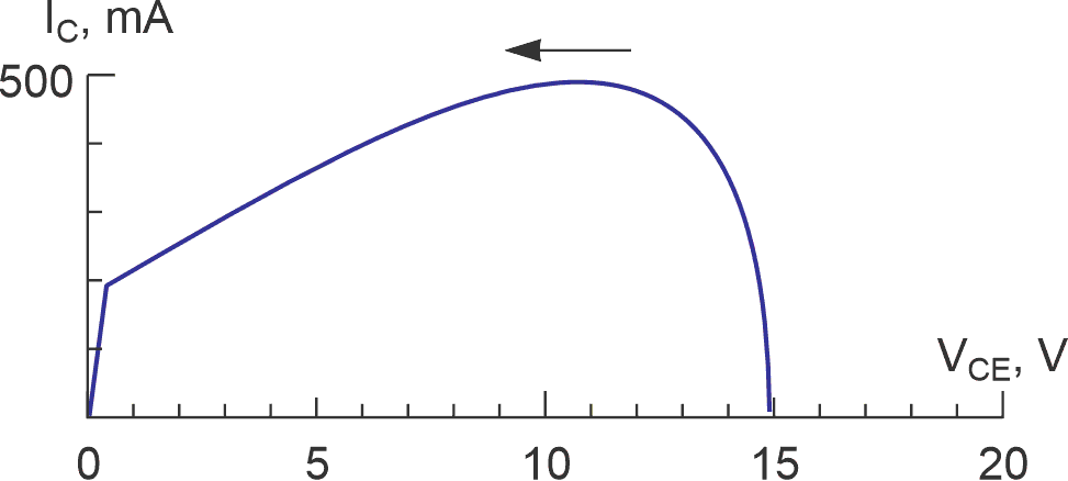
Having constructed a Lissajous pattern of VCE versus IC as shown in Figure 2, we process that pattern.
 |
|
| Figure 2. | The voltage versus current Lissajous pattern for Q1. |
Just one comment about obtaining that Lissajous pattern. The oscilloscope simulations in the Multisim-SPICE I was using do not support “x” versus “y” capability, and therefore cannot provide the Lissajous pattern. I made the pattern you see here by reading out the voltage and current values at each time step of the oscilloscope display and then plotting them using GWBASIC. There were 240 datums for each, a total of 480 readings, which were pretty tedious to acquire. Ordinarily, I can’t concentrate on work and listen to music at the same time, but this time, listening to some Petula Clark recordings through all of this did help to ease the monotony.
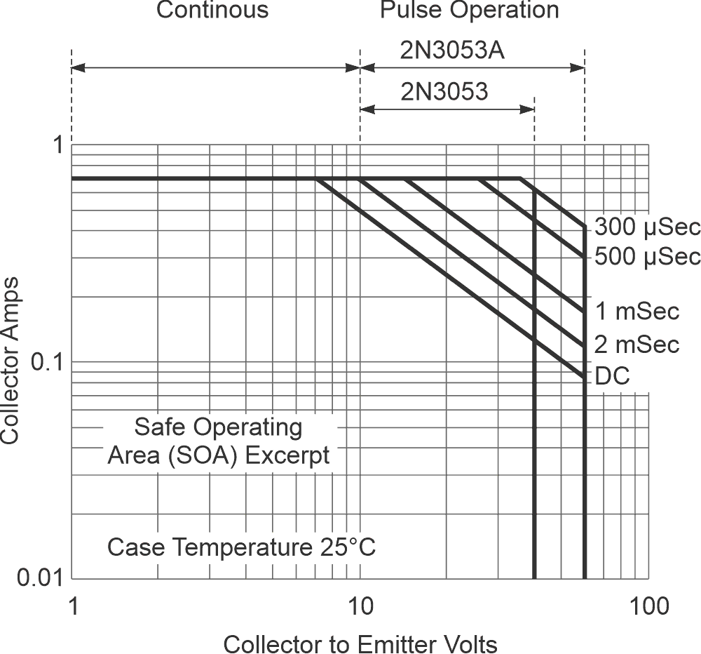
In all my years of acquaintance with the 2N2222, I have never seen any specification or any datasheet that presented the SOA boundaries for that device. In fact, I’ve never seen the SOA boundaries for any TO-18 packaged device. In the TO-5 and TO-39 packages, the one and only time I have ever come across SOA boundary information was for the 2N3053 and 2N3053A, and even today, some datasheets omit that information.
As a result, we just have to make do with what we’ve got, which for now is this partial reconstruction of the 2N3053 and 2N3053A SOA chart taken from a very old datasheet from RCA that I stashed away long ago (Figure 3).
 |
|
| Figure 3. | Safe operating area reconstruction of the 2N3053 and 2N3053A SOA chart taken from a very old datasheet from RCA. |
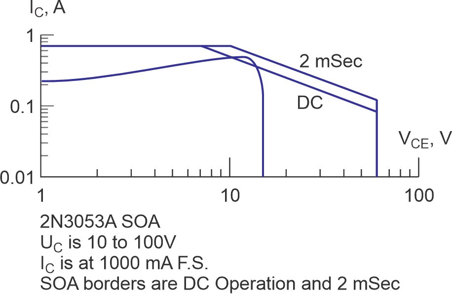
We replot the VCE versus IC data using logarithmic scaling, and then we overlay that result with the SOA boundaries of our NPN, but we encounter a difficulty (Figure 4).
 |
|
| Figure 4. | SOA examination using logarithmic scaling. |
The 2N2222 has a peak power rating of 1.2 watts, while the 2N2219, a first cousin to the 2N2222, has a peak power rating of 3 watts, versus a 7 watts rating for the 2N3053. I would therefore imagine that the 2N2222 SOA boundaries are quite a bit lower than those of the 2N3053. We note that the SOA curve of Q1 operating in this circuit moves outside of the DC operating boundary for the 2N3053 and thus, in all likelihood, it moves well outside of the 2N2222 equivalent limits.
Voltage and current excursions toward the upper right of this diagram are NOT a good thing.
The 2N2222 as used here can well be expected to fail, maybe sooner, maybe later, but it is set up for eventual calamity. Regardless of other factors that may apply to this design, remedial SOA measures should be considered.
The first is to reduce the capacitance of C1 (Figure 5).
 |
|
| Figure 5. | The effects of reducing the capacitance of C1. |
Using a smaller value of C1, or perhaps using no C1 at all, will lower the peak collector current and will make the switching events occur more quickly. This will take us away from the upper right corner of the SOA plot, and from that standpoint, this is a very good thing to do.
Adding R3, as shown in Figure 6, can also reduce the peak collector current.
 |
|
| Figure 6. | The effects of including a collector resistance. |
Although using R3 will slow down the C1 discharge rate for each discharge event, doing so will keep the peak collector current down, and that is a desirable SOA outcome.
If, for some reason, C1 has to be there, omitting R3 is not a good idea.