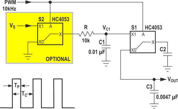
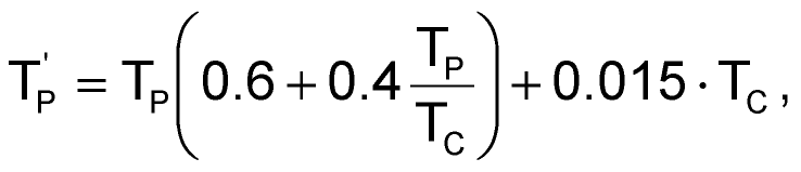
The enduring simplicity of PWM DACs will always earn them a place in the designer’s cookbook, but slow response time and the problem of PWM ripple tend to limit their appeal and utility. The usual way of attenuating PWM ripple, an RC low pass filter, can never succeed in completely eliminating it, and only makes output settling time agonizingly slow if you try. Figure 1 shows a different approach, which can overcome these drawbacks – using a synchronous S&H (sample & hold).
 |
||
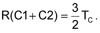
| Figure 1. | S1’s sample-hold operation eliminates PWM ripple. | |
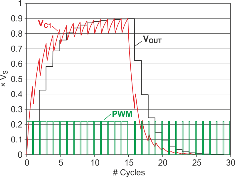
The Design Idea relies on the inherently periodic nature of PWM ripple, which makes it have exactly the same voltage at any synchronously chosen point in the VC1 waveform, as shown in Figure 2. Therefore, if VC1 is synchronously sampled, as by Figure 1’s analog switch S1 and transfer capacitance C2, then held (hence Sample-and-Hold) to produce output VOUT as by C3, the result will be a smooth, ripple-free VOUT regardless of how large the AC component at VC1 might be. This is illustrated in the plots of DAC dynamic behavior in Figure 2.
 |
||
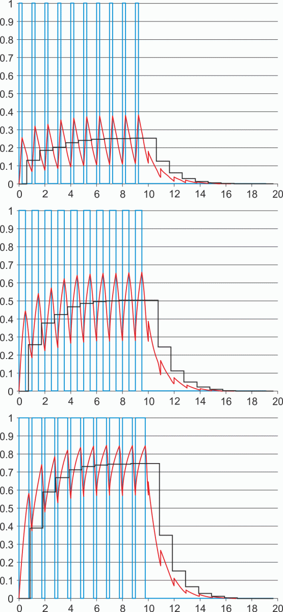
| Figure 2. | DAC settles to 8-bit accuracy in under 15 PWM cycles. | |
Moreover, because synchronous sampling inherently eliminates ripple independent of how short the RC1 time constant may be, it follows that the RC1 product can be made quite short indeed. This can dramatically cut settling time, as in Figure 1, where RC1 = 100 µs = TC = the PWM period, resulting in settling (to 8-bit precision) in less than 15·TC = 1.5 ms for the example case. But of course, as with all good things, we know there must a limit. So the question becomes: How short can RC1 be made consistent with proper DAC function, and what design factors set that limit?
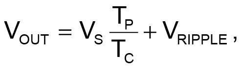
A closer look at the VC1 waveform suggests the answer: VOUT is sampled, not from the average value of VC1, but from the ripple maxima. Therefore:
With…
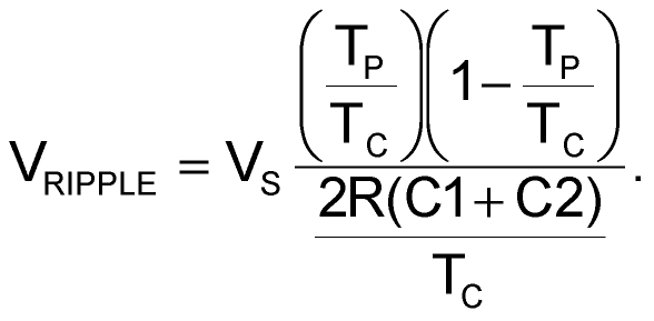
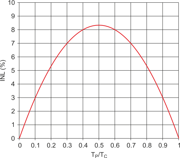
Summing this non-linear component with the DAC VOUT function therefore makes the DAC transfer function nonlinear too, resulting in an integral nonlinearity (INL) error that, with the example circuit constants, can be as large as 8.3% of full-scale (Figure 3). For many applications, this much INL would be unacceptable. Fortunately, there’s a simple (software) fix: Numerical pre-emphasis of the DAC setting. For example, using the constants of Figure 1, where…
If we alter TP …
the VRIPPLE term will disappear from VOUT and 8-bit INL is restored.
 |
||
| Figure 3. | INL Error caused by rectified ripple. | |
It’s worth mentioning the “optional” elements VS and S2 which generate the RC1 input waveform from a precision reference (VS), and thus avoid superimposing the noise and dodgy regulation often characteristic of logic power supplies (and therefore riding on the PWM logic signal) on VOUT. Of course if the accuracy requirements of your application are sufficiently undemanding to make this unnecessary, they can be omitted, and R simply connected directly to the PWM signal.
Worth mentioning because, as I said at the outset, enduring simplicity is one of the main charms of PWM DACs!
 |
||
| Figure 4. | DAC responses at three different output settings. | |