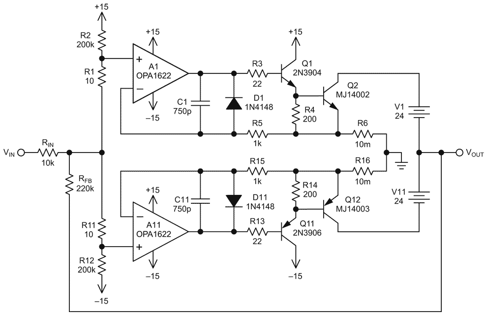
Inspired by the excellent idea shown in the article “Class AB 20-W current booster is insensitive to temperature variations” by Jordan Dimitrov (Ref. 1), this variation of the design shown in Figure 1 enables an amplifier that can deliver higher output voltage swings while still using standard (e.g., ±15-volt) op amps at the front end.
 |
|
| Figure 1. | Schematic of high output voltage swing current booster. Higher swing is provided by using floating power supplies and taking the output from the collectors of the output transistors. Note global feedback in order to close the loop around the output stage. |
This does require the use of two floating power supplies on the output and modern power supply technology makes this easy for OEMs. This author has found that an excellent DIY option is standard server power supplies available in 12-, 24-, and 48-volt versions at very low cost and high wattages. For DIY usage the lowest cost option is often satisfied by refurbished supplies.
This circuit takes its output from the collector (or drain if MOSFETs are used) with the center tap of the two output stage power supplies providing the output node. This configuration provides voltage gain in the output stage to develop the necessary output voltage swing from the ±15-volt op amps at the input.
The current drive configuration operates identically to the previously mentioned circuit with this example re-scaled in component values to provide higher currents. Re-scaling of the output stage values resulted in 75 mA quiescent current in the output transistors.
The example circuit shows a pair of TI OPA1622 amplifiers only because the author did not have any of the OPA2991 used in the previous article but either amplifier can be used (and the OPA2991 has the advantage of being a dual).
This circuit was tested up to 30 watts (8 Ω load with a ±24-volt output stage). Global negative feedback, in this case designed for an overall gain of 20, is required with the collector output along with additional compensation. Rate-of-closure techniques were used to arrive at the compensation shown. An inverting circuit is the simplest configuration, although it places limits on how high the input impedance can be, in this case it is 10 kΩ, sufficient for most applications.
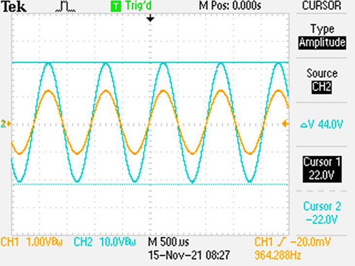
Figure 2 shows VIN (the yellow trace) and VOUT (the blue trace) at 1 kHz.
 |
|
| Figure 2. | Input and output waveforms at 1 kHz. |
Figure 3 shows their spectrums at maximum power and 1 kHz.
|
|||
| Figure 3. | FFT of input (a) and output (b). | ||
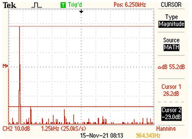
An astute observer would question how the input appears to have a larger proportion of the second harmonic. This author triple checked this setup and at this moment can only conclude that the input FFT is suffering from limitations (e.g., noise floor) of the oscilloscope itself.
References
- Class AB 20-W current booster is insensitive to temperature variations (EDN, Jordan Dimitrov)
- Phase Margin Estimation Using the Rate-of-Closure (All About Circuits, Dr. Sergio Franco)
- Op amp stability – Part 2 (TI Precision Labs)
- Stability for Power Operational Amplifiers (Apex Microtechnology)
- Simple, precise, bi-directional current source (EDN, Jerry Steele)