This Design Idea builds on a previous one (Reference 1) to realize a precision peak detector with a bandwidth of 15 to 30 MHz or more, depending on the maximum input-signal level of your application. The crucial feature of this Design Idea is an ultrafast comparator that provides the high slew rate and low propagation delay that this application requires. The comparator in this design is the Analog Devices AD8561, a 7-nsec device. This peak detector provides accuracy from 100 Hz to more than 14 MHz at input-signal levels of 100 mV p-p to 6 V p-p. At higher frequencies, the maximum usable input-signal level decreases. The circuit exhibits an accuracy of ±3% over much of the input-level range. Also, its high input impedance of about 100 kΩ in parallel with 3 pF does not significantly load the circuit under test in many applications; 3 pF results in an impedance of 3.5 kΩ at 15 MHz.
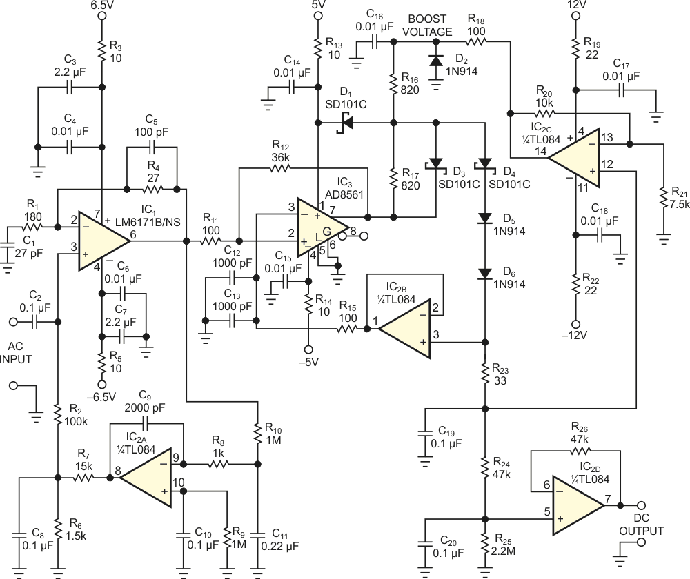
Referring to Figure 1, the high-input-impedance buffer comprising IC1 and its associated components provides the ac signal to the ultrafast comparator, IC3. The output of IC1 centers on 0 V dc by the action of op amp IC2A and its associated components, which sample the dc level at Pin 6 of IC1 and then provide a dc-correction voltage to Pin 3 of IC1. This action virtually eliminates the effects of IC1’s input-offset voltage and input-bias currents. R1, R4, and C1 provide a small amount of gain boost as the frequency increases to 25 MHz, and C5 then begins to roll off the gain.
 |
|
| Figure 1. | This precision peak detector uses an ultrafast comparator to achieve high accuracy over a wide input-frequency range. |
The input signal capacitively couples to the input buffer, so, for proper operation, the input-ac signal must have a symmetrical waveform, such as a sine wave. An unsymmetrical waveform has a shift in its peak value after passing through C2, and, as a result, the output of the peak detector will be inaccurate. The output of comparator IC3 swings high when the input at Pin 2 is higher than the dc level at Pin 3. This action, in turn, charges holding capacitor C19 through R17, D4, D5, D6, and R23. When the voltage on C19 is higher than the peak signal level at Pin 2 of IC3, the comparator stops providing charging pulses at its output. At equilibrium, the comparator provides output pulses with the correct amplitude and width to maintain the voltage on C19 at approximately the peak level of the input signal. The high-input-impedance dc buffer, IC2B, minimizes the discharging of C19 between charging pulses.
The network comprising R24, R25, and C20 filters and attenuates the dc output by 2.1%. This attenuation is necessary because the output tends to be slightly higher than the actual peak level of the input signal at Pin 3 of IC1. The circuitry comprising IC2C and its associated components provides a novel feature: a voltage boost at Pin 14 of IC2C as the voltage on holding capacitor C19 increases. The circuitry then applies this voltage boost to R16, which in turn causes the voltage swing at the junction of R16 and R17 to increase as the charge on C19 increases. This action causes the amplitude of the pulses driving D4 to increase. This action maintains a relatively constant drive to C19 as its charge increases.
Diode D1 keeps the voltage at the output of IC3 from exceeding its supply voltage. Diode D2 keeps the boost voltage from going to a large negative level at start-up, which could cause the circuit to latch up. The switching action of the comparator and diode D3 prevents latch-up due to a large positive-boost transient. This circuit exhibits no indication or tendency for instability. The maximum input signal is 6 V p-p because of the input common-mode-voltage specification of the AD8561 comparator. The supply voltages for the input buffer are ±6.5 V to avoid the possibility of severely overdriving the comparator.
You can improve the precision of the circuit by substituting a 100-kΩ potentiometer for R4 to provide an output-level adjustment, and a dc-offset adjustment would improve accuracy at low signal levels.
| Table 1. | Measured results for wideband peak detector | ||||||||||||||||||||||||||||||||||||||||||||||||||||||||||||||||||||||||||||||||||||||||||||||||||||||||||||||||||||||||||||||||||||||||||||||||||||||||||
|
|||||||||||||||||||||||||||||||||||||||||||||||||||||||||||||||||||||||||||||||||||||||||||||||||||||||||||||||||||||||||||||||||||||||||||||||||||||||||||
This circuit used a 300-MHz-bandwidth oscilloscope to make the performance measurements. As a result, the data in Table 1 may include some measurement errors. Therefore, take the results in the table as representing the circuit’s performance rather than as precise data. The data is simply the result of the best equipment on hand when the measurements were made.
Reference
- Jim McLucas, “Precision peak detector uses no precision components“.