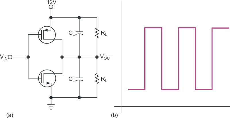
Many PWM (pulse-width-modulated) applications, such as Class D audio amplifiers, require symmetric drive circuitry. Comprising complementary N- and P-channel FET devices with gates and sources connected, the textbook CMOS pair in Figure 1 provides a low-impedance path to either the positive or the negative power supply and can directly drive a logic-level N-channel FET. Direct coupling of the CMOS pair to the logic driver works well in PWM systems in which the controlled devices operate at the same voltage as the logic circuits. However, raising the output FETs' power-supply voltage while driving the gates from lower voltage logic results in the P-channel device's remaining in conduction because of the difference between supply voltages.
 |
|
| Figure 1. | The textbook complementary-CMOS pair (a) produces a clean output waveform with fast on/off transitions (b). |
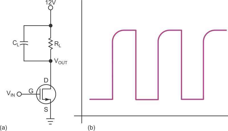
To achieve an off-state, an amplifier's P-channel FET's gate must go to the positive-supply rail. Complementary-CMOS logic-level drivers can't accommodate the amplifier's high positive-supply voltage, and alternatives, such as using commercial FET drivers and operational-amplifier level-shift circuits, add cost and complexity. You can add an external high-voltage N-channel FET to drive the P-channel- amplifier FET's gate (Figure 2). However, capacitive loading imposes an exponential-rise characteristic on the drive waveform, leaving the P-channel FET in its linear operating region for an extended period and thus limiting switching frequency and causing significant power losses in the cascaded FETs.
 |
|
| Figure 2. | An N-channel FET driver (a) has output that exhibits an exponential rising edge on shutoff (b). |
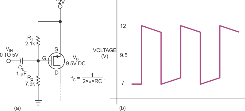
Current-generation PWM systems can operate at relatively high switching frequencies and, as Figure 3 shows, allow you to use a dc-blocking coupling capacitor, CB, between the logic-level driver's output and the P-channel output FET's gate. Resistive divider R1 and R2 applies a dc bias to the output FET's gate that's equal to the difference between the output power-supply voltage and the midrail logic voltage. For example, in a 12 V Class D PWM audio amplifier driven from a 5 V microcontroller, bias the P-channel FET's gate at 9.5 V (12 V – 5 V/2). Use the specified FETs for logic-level gate drive as output devices because other FETs don't exhibit nominal IDS characteristics at gate drives of 5 V or lower.
 |
|
| Figure 3. | Adding resistive bias and capacitive coupling to an N-channel MOSFET (a) improves transition times but introduces waveform droop during on or off intervals (b). |
 |
|
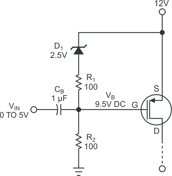
| Figure 4. | Inserting a zener diode into the bias divider allows optimization of the coupling capacitor’s value and the P-channel device’s bias voltage for logic-level drive. |
Battery-powered amplifiers with resistive-divider output-stage bias introduce an additional complication. As battery voltage decreases, so does bias. Instead, you can use a voltage-reference IC or a zener diode, D1, to provide a constant bias voltage regardless of supply-voltage variations (Figure 4). This technique consumes less power than a purely resistive divider and offers more flexibility in coupling-capacitor selection to reduce waveform droop. Based on Texas Instruments' TPA2010 PWM power-amplifier IC, a Class D audio power amplifier boosts the TPA2010's 2.5 W differential output to more than 200 W rms into an 8 Ω load (Figure 5).
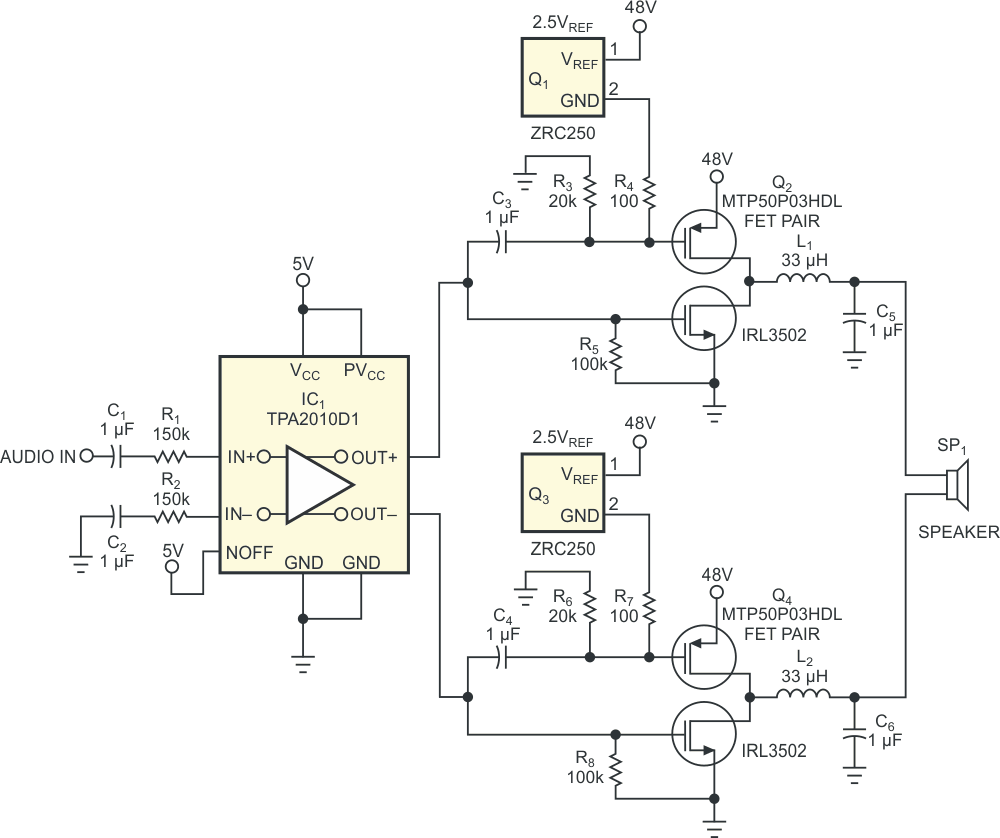 |
|
| Figure 5. | This Class D audio amplifier boosts its driver’s output to 200 W rms for a 48 V power supply. |