One classic set you’ll see in most гvintage mystery movies is an interrogation room with a “two-way” mirror in one wall. This cool gadget lets the witnesses see the suspects from another room while the suspects can see only themselves. Which direction the two-way mirror works in is determined by which side has more light. The bright side is the suspect’s mirror. The dim side is the witness’s window.
So, what does that have to do with electronics?
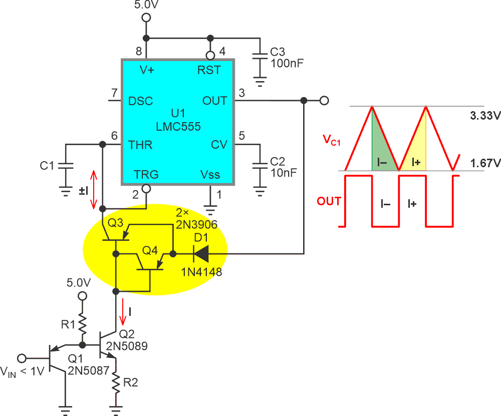
This simple design idea describes a two-way current mirror that, in dubious analogy to the optical kind, can mirror or transmit according to whether the input or output side is more positive. It comprises just two BJTs and one diode and is highlighted yellow in Figure 1’s 555 triangle wave VCO.
 |
|
| Figure 1. | D1, Q3, and Q4 comprise the two-way current mirror. It passively conducts Q2’s collector current to C1 via Q3’s base-collector when OUT versus C1 is negative, but becomes an active inverting unity-gain current source when OUT goes positive and reverses the polarity. |
Here’s how it works.
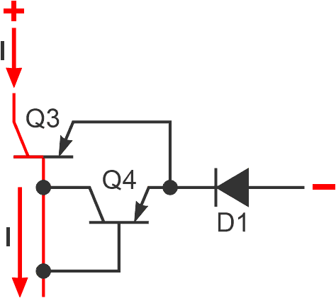
Let’s call the D1 node the input, and the C1 node the output. When U1’s OUT pin is low, D1 and the mirror are reversed biased. Now, Q2’s collector current I has nowhere to go except to forward-bias Q3’s base-collector junction, as shown in Figure 2. This connects Q2 to C1 so current I linearly ramps C1 negative.
 |
|
| Figure 2. | When OUT goes low, Q4 is off while Q3 saturates and transmits negative current I to C1. Keep VIN < 1 V so Q2 won’t saturate. |
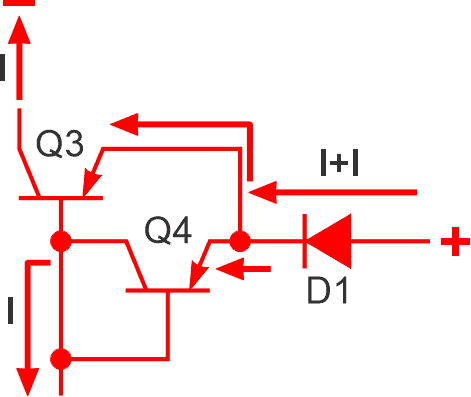
When C1 descends to U1’s trigger voltage (1.33 V), OUT transitions positive. This swaps polarity across the mirror, forward biasing it, pulling the emitters of Q3 and Q4 positive relative to C1. Q3 and Q4 then assume the role of a normal active unity-gain current mirror. They now mirror an inverted positive version of I to C1, making it ramp positive, as shown in Figure 3.
 |
|
| Figure 3. | With OUT high, the mirror goes active and inverts I into a positive current to charge C1. |
When C1 charges up to U1’s threshold (3.67 V), OUT snaps negative again and a new oscillation cycle begins, finishing output of a (theoretically) symmetrical isosceles triangle waveshape. Keep VIN < 1 V.
Details, including strengths and weaknesses, of the classic two-transistor current mirror can be found in numerous electronics design references (Ref. 1).
Of course, a complementary version of the two-way mirror could also be made with NPN transistors. If a current source replaces Q2’s current sink, it will work equally well.
You might be wondering what’s D1 for? When OUT goes low, both transistor emitters are reverse-biased, so no current should flow through the input node anyway.
Therefore, D1 is superfluous, right?
Well, no, it isn’t. The reason is summed up in the term “reverse beta.” It turns out that when you reverse-bias a BJT’s base-emitter junction and forward-bias its base-collector, significant current flow is possible – even likely – from collector to emitter. The associated current gain of this upside-down configuration is always way lower than normal beta, but it’s still more than leakage and definitely too significant to ignore. We need D1.
That wraps up the whodunit of the two-way current mirror. Thanks for reading. Sorry if it’s old news to you. It was new news to me when I thought of it, and I hope to show more applications for it in the near future.