The TL431 has been around for nearly 50 years. During those decades, while primarily marketed as a precision adjustable shunt regulator, this legacy device also found its way into alternative applications. These include voltage comparators, audio amplifiers, current sources, overvoltage protectors, etc. Sadly, in almost every example from this mighty menagerie of circuits, the 431’s “anode” pin sinks to the same lowly fate. It gets grounded.
Current sink regulation
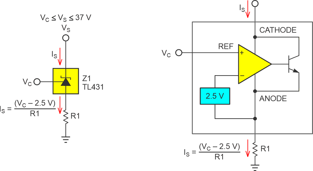
The design idea presented here offers that poor persecuted pin a more buoyant role to play, Figure 1.
 |
|
| Figure 1. | The floated anode serves as a sense pin for active current sink regulation. |
The Figure 1 block diagram shows how the 431 works at a conceptual level where:
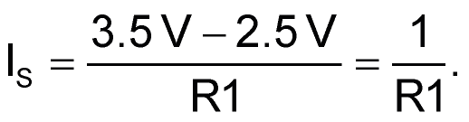
as VC = 2.5 V to 3.5 V;
VS < 37 V, IS < 100 mA, IS(VS – R1·IS) < 500 mW @ 50 °C ambient.
Series connection adds an internal 2.5-V precision reference to external voltage input on the ANODE pin. The op-amp subtracts this sum from the voltage input on the REF pin, then amplifies and applies the difference to the pass transistor. If the difference is positive (sum < REF), the transistor turns on and shunts current from CATHODE to ANODE. Otherwise (sum > REF), it turns off.
If the 431 is connected in the traditional fashion (REF connected to CATHODE and ANODE grounded). In that case, the scheme works like a shunt voltage regulator should, forcing CATHODE to a resistor-string-programmed multiple of the internal 2.5-V reference voltage. But what will happen if the REF pin is connected to a constant control voltage (VC > 2.5 V); and the ANODE, instead of being grounded, floats freely on current sensing resistor R1?
What happens is the current gets regulated instead of the voltage. Because VC is fixed and can’t be pulled down to make REF = ANODE + 2.5, ANODE must be pulled up until equality is achieved. For this to happen:
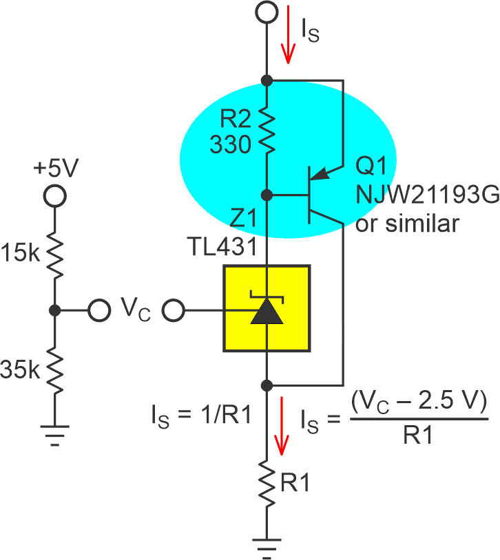
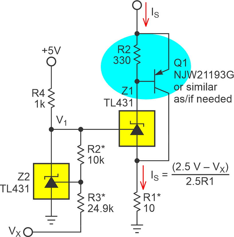
Constant current sink regulation of 1/R1
 |
|
| Figure 2. | Booster transistor Q1 can handle current and voltage beyond 431 max IC and dissipation limits, while the 3.5-V voltage divider programs a constant IS. |
Figure 2 illustrates how a fixed voltage divider might be used (assuming a 5-V rail that’s accurate enough) to use a floated-anode Z1 to regulate a constant sink current of:
It also illustrates adding a booster transistor Q1 to accommodate applications needing current or power beyond Z1’s modest TO92ish limits. Notice that Z1’s accuracy will be unimpaired because whatever fraction of IS that Q1 causes to bypass Z1 is summed back in before passing through R1.
Programming sink current with DAC
 |
|
| Figure 3. | DAC control of IS, the DAC signal is inverted, while Z2 provides the necessary level shift. |
Figure 3 shows how IS might be digitally programmed with a 2.5-V DAC signal. Note the DAC signal is inverted (IS = max when VX = 0) while Z2 provides the necessary level shift:
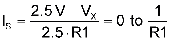
as VX = 2.5 V to 0.
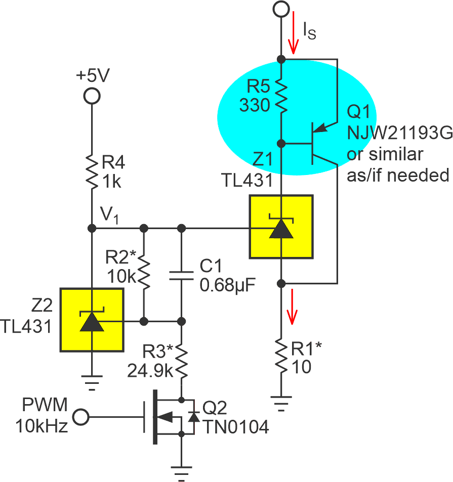
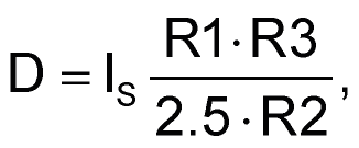
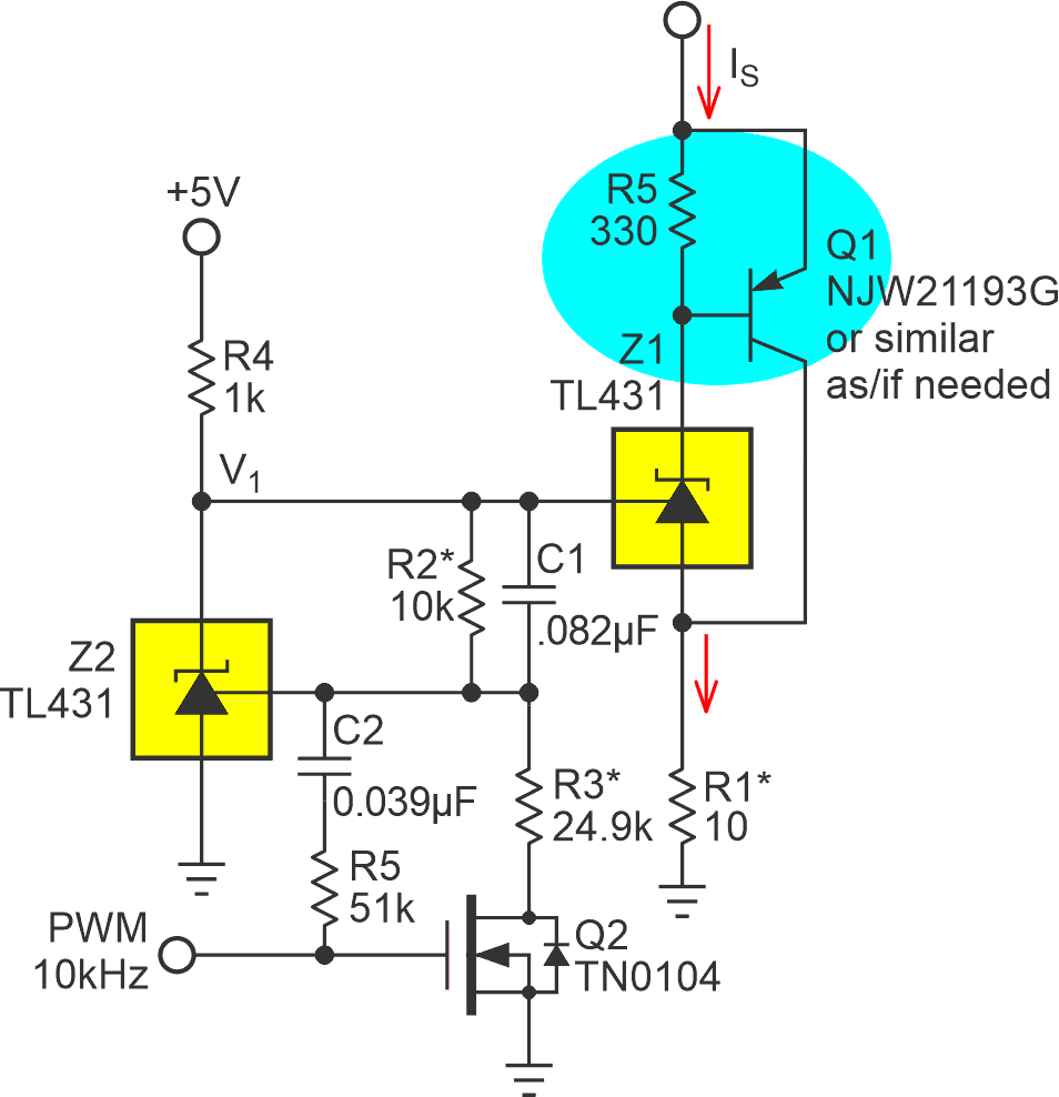
Programming sink current to D/R1 with DAC
 |
|
| Figure 4. | PWM control of IS, where IS is the ratio of the PWM duty factor and R1. |
Figure 4 shows an alternate programming method using PWM with IS = D/R1 where D equals the 0 to 1 (0% to 100%) PWM duty factor:
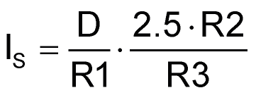
as D = 0 to 1

The 8-bit PWM resolution and 10-kHz frequency are assumed. The R2C1 single-pole ripple filter has a time constant of approximately 64x the PWM period (10 kHz = 100 µs assumed) for 1-lsb peak-to-peak max ripple and 38-ms max settling time.
Speeding up settling time
One shortcoming of Figure 4 is the long settling time (~40 ms to 8 bits) imposed by the single-pole R1C12 ripple filter. If an extra resistor and capacitor won’t break the bank, that can be sped up by a factor of about 5 (~8 ms) with Figure 5’s R5C2 providing 2nd-order analog-subtraction filtration (Ref. 1).
 |
|
| Figure 5. | The addition of R5 and C2 provides faster settling times with a 2nd-order ripple filter. |
Programmable current sink application circuit
Finally, Figure 6 shows the Figure 4 circuit combined with an inexpensive 24-W AC adapter and a 5-V regulator to power a small digital testing system. Be sure to adequately heatsink Q1.
 |
|
| Figure 6. | The combined current sink and small system power supply where the max IS is 1 A, Max VS is 20 V, and IS = D. |
Reference
- Woodward, Stephen. "Cancel PWM DAC ripple with analog subtraction."