“Gold-plated” without the gold plating
Alright, I admit that the title is a bit over the top. So, what do I mean by it? I mean that:
- The application of PWM control to a regulator does not significantly degrade the inherent DC accuracy of its output voltage,
- Any ability of the regulator’s output voltage to reach below that of its internal reference is supported, and
- This is accomplished without the addition of a new reference voltage.
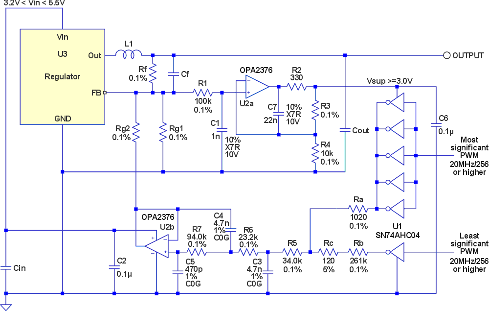
Refer to Figure 1.
 |
|
| Figure 1. | This circuit meets the requirements of “Gold-Plated PWM control” as stated above. |
How it works
The values of components CIN, COUT, CF, and L1 are obtained from the regulator’s datasheet. (Note that if the regulator is linear, L1 is replaced with a short.)
The datasheet typically specifies a preferred value of RG, a single resistor between ground and the feedback pin FB.
Taking the DC voltage VFB of the regulator’s FB pin into account, R3 is selected so that U2A supplies a VSUP voltage greater than or equal to 3.0 V. C7 and R3 ensure that the composite is non-oscillatory, even with decoupling capacitor C6 in place. C6 is required for the proper operation of the SN74AC04 IC U1.
The following equations govern the circuit’s performance, where VMAX is the desired maximum regulator output voltage:
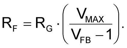
They enable the regulator output to reach zero volts (if it is capable of such) when the PWM inputs are at their highest possible duty cycle.
U1 is part of two separate PWMs whose composite output can provide up to 16 bits of resolution. RA and RB + RC establish a factor of 256 for the relative significance of the PWMs.
If eight bits or less of resolution is required, RA and RB, and the least significant PWM, can be eliminated, and all six inverters can be paralleled.
The PWMs’ minimum frequency requirements shown are important because when those are met, the subsequent filter passes a peak-to-peak ripple less than 2–16 of the composite PWM’s full-scale range. This filter consists of RA, RB + RC, R5 to R7, C3 to C5, and RA and U2B.
Errors
The most stringent need to minimize errors comes from regulators with low and highly accurate reference voltages. Let’s consider 600 mV and 0.5% from which we arrive at a 3-mV output error maximum inherent to the regulator. (This is overly restrictive, of course, because it assumes zero-tolerance resistors to set the output voltage. If 0.1% resistors were considered, we’d add 0.2% to arrive at 0.7% and more than 4 mV.)
Broadly, errors come from imperfect resistor ratios and component tolerances, op-amp input offset voltages and bias currents, and non-linear SN74AC04 output resistances. The 0.1% resistors are reasonably cheap.
Resistor ratios
If nominally equal in value, such resistors, forming a ratio, contribute a worst-case error of ±0.1%. For those of different values, the worst is ±0.2%. Important ratios involve:
- RG1, RG2, and RF;
- R3 and R4;
- RA and RB + RC.
Various RF, RG ratios are inherent to regulator operation.
The RG1, RG2; R3, R4; and RA, RB + RC pairs have been introduced as requirements for PWM control.
The RA/(RB + RC) error is ±0.2%, but since this involves a ratio of 8-bit PWMs at most, it incurs less than 1 least significant bit (LSbit) of error.
The RG1, RG2 pair introduces an error of ±0.2 % at most.
The R3, R4 pair is responsible for a worst-case ±0.2 %. All are less than the 0.5% mentioned earlier.
Temperature drift
The OPA2376 has a worst-case input offset voltage of 25 µV over temperature. Even if U2A has a gain of 5 to convert FB’s 600 mV to 3 V, this becomes only 125 µV.
Bias current is 10-pA maximum at 25 °C, but we are given a typical value only at 125 °C of 250 pA.
Of the two op-amps, U2B sees the higher input resistance. But its current would have to exceed 6 nA to produce even 1-mV of offset, so these op-amps are blameless.
To determine U1’s output resistance, its spec shows that its minimum logic high voltage for a 3-V supply is 2.46 V under a 12-mA load. This means that the maximum for each inverter is 45 Ω, which gives us 9 Ω for five in parallel. (The maximum voltage drop is lower for a logic low 12 mA, resulting in a lower resistance, but we don’t know how much lower, so we are forced to worst-case it at a ridiculous 0 V!)
Counting C3 as a short under dynamic conditions, the five inverters see a 35-kΩ load, leading to a less than 0.03% error.
Wrapping up
The regulator and its output range might need an even higher voltage, but the input voltage VIN has been required to exceed 3.2 V. This is because U1 is spec’d to swing to no further than 80 mV from its supply rails under loads of 2 kΩ or more.
(I’ve added some margin, but it’s needed only for the case of maximum output voltage.)
You should specify VMAX to be slightly higher than needed so that U2B needn’t swing all the way to ground. This means that a small negative supply for U2 is unnecessary. IN must also be less than 5.5 V to avoid exceeding U2’s spec. If a larger value of VIN is required by the regulator, an inexpensive LDO can provide an appropriate U2 supply.
I grant that this design might be overkill, but I wanted to see what might be required to meet the goals I set. But who knows, someone might find it or some aspect of it useful.