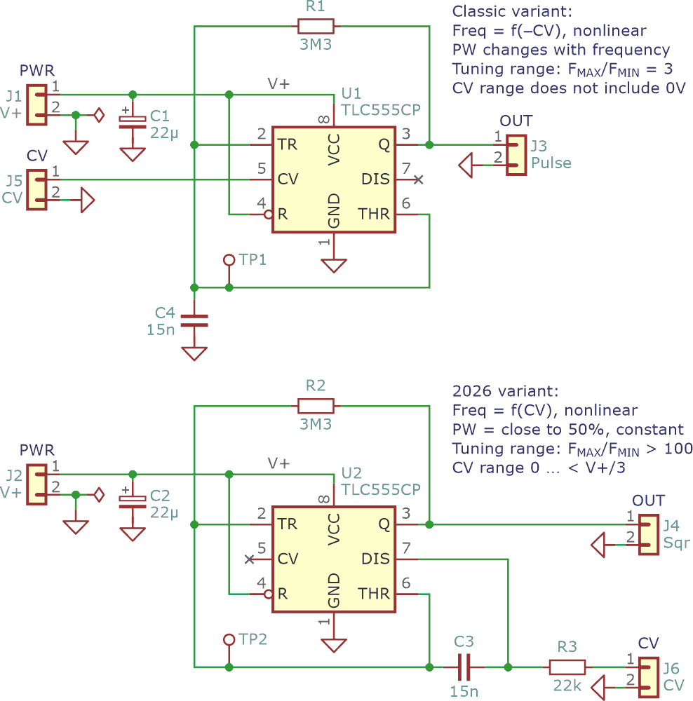
It is well known that a 555 timer in astable mode can be frequency modulated by applying a control voltage (CV) to pin 5. The schematic on the top of Figure 1 shows this classic 555 VCO.
Modulating pin 5 has some severe drawbacks: The control voltage (CV) must be significantly > 0 V and < V+, otherwise the oscillation stops.
In contrast to a typical VCO, which outputs 0 Hz or FMIN @ CV = 0 and reaches FMAX @ CVMAX, the CV behavior of the classic 555 VCO is inverted and nonlinear. This is due to the modulation of the upper and lower Schmitt trigger thresholds, and pulse width changes with frequency. The useful tuning range FMAX/FMIN is limited to about 3.
Stephen Woodward’s “Can a free-running LMC555 VCO discharge its timing cap to zero?” (Ref. 1) shows some clever improvements: linear-in-pitch CV behavior and an extended 3 octave range, but still suffers from other “pin 5” drawbacks.
The schematic on the bottom of Figure 1 shows a new variant of the 555 VCO. Pin 5 is not modulated, which leads to a constant 50% pulse width, independent of frequency.
 |
|
| Figure 1. | Classic VCO (top) and new 555 VCO variant (bottom), where Pin 5 is not modulated, which leads to a constant 50% pulse width, independent of frequency. |
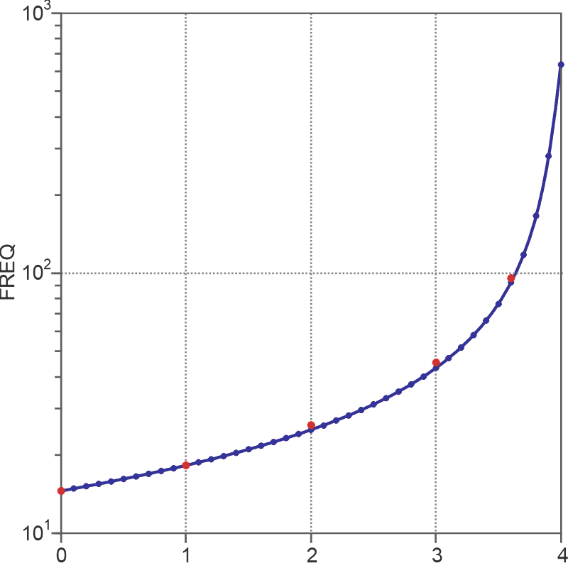
A rising CV results in a higher frequency. CV = 0 is allowed and generates FMIN.
The useful tuning range is > 10 and ≥ 100, with some caveats noted below.
Although it uses only 2 resistors and 1 capacitor, like the classic 555 astable configuration, it is a bit harder to understand. The basic function of adding a fraction of the square wave output voltage to the triangle voltage over C, which rises in frequency, is described in my recent Design Idea (DI), “Wide-range tunable RC Schmitt trigger oscillator” (Ref. 2).
There, I use a potentiometer to add a fraction of the output to the capacitor voltage.
In the new 555 VCO variant, the potentiometer voltage is replaced by an external CV, which is chopped by the 555 discharge output (pin 7).
When CV is 0, the voltage on the right side of C3 is also 0, and the VCO outputs FMIN. With rising CV, a square wave voltage between 0 V (pin 7 discharging) and CV (pin 7 open) appears on the right side of C3. Similar to my above-mentioned DI, this square wave voltage must always be smaller than the hysteresis voltage (555: VH = V+/3), otherwise FMAX goes towards infinity. That is why you must watch your CVMAX if you want to reach high FMAX/FMIN ratios.
Figure 2 shows a QSPICE simulation of frequency with respect to CV from 0 V to 3.9 V in 100 mV steps.
 |
|
| Figure 2. | QSPICE simulation of frequency with respect to CV from 0 V to 3.9 V in 100 mV steps. |
A prototype with component values from Figure 1 and V+ = 12 V has been breadboarded, and a rough frequency-versus-CV curve is measured and marked with a red dot in the QSPICE simulation in Figure 2.
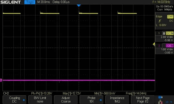
Figure 3 shows a scope screenshot for FMIN.
 |
|
| Figure 3. | A scope screenshot for FMIN, CH1 (yellow) output voltage, CH2 (magenta) CV=0. |
In conclusion, the new 555 VCO circuit overcomes some drawbacks of the classic version, like limited CV range, inverted CV/Hz behavior, and changing pulse width, without using more components. Unfortunately, it still shows nonlinear CV/Hz behavior. Maybe using a closed loop, with an opamp and a simple charge pump, can tame it by raising the chip count to 2.
References
- Woodward, Stephen. "Can a free running LMC555 VCO discharge its timing cap to zero?"
- Schüler, Uwe. "Wide-range tunable RC Schmitt trigger oscillator."