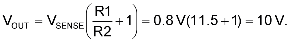
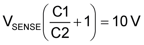
The typical regulator output network
Many voltage regulator chips, both linear and switching, use the same basic two-resistor network for output voltage programming. Figure 1 illustrates this feature in a typical switching (buck type) regulator, see R1 and R2, where:
Quantitatively, the VSENSE feedback node voltage varies from type to type and recommended values for R1 can vary too, but the topology doesn’t. Most conform faithfully to Figure 1. This de facto uniformity is useful if your application involves PWM control of VOUT.
 |
|
| Figure 1. | A typical regulator output programming network where the VSENSE feedback node and values for R1 varies from type to type. |
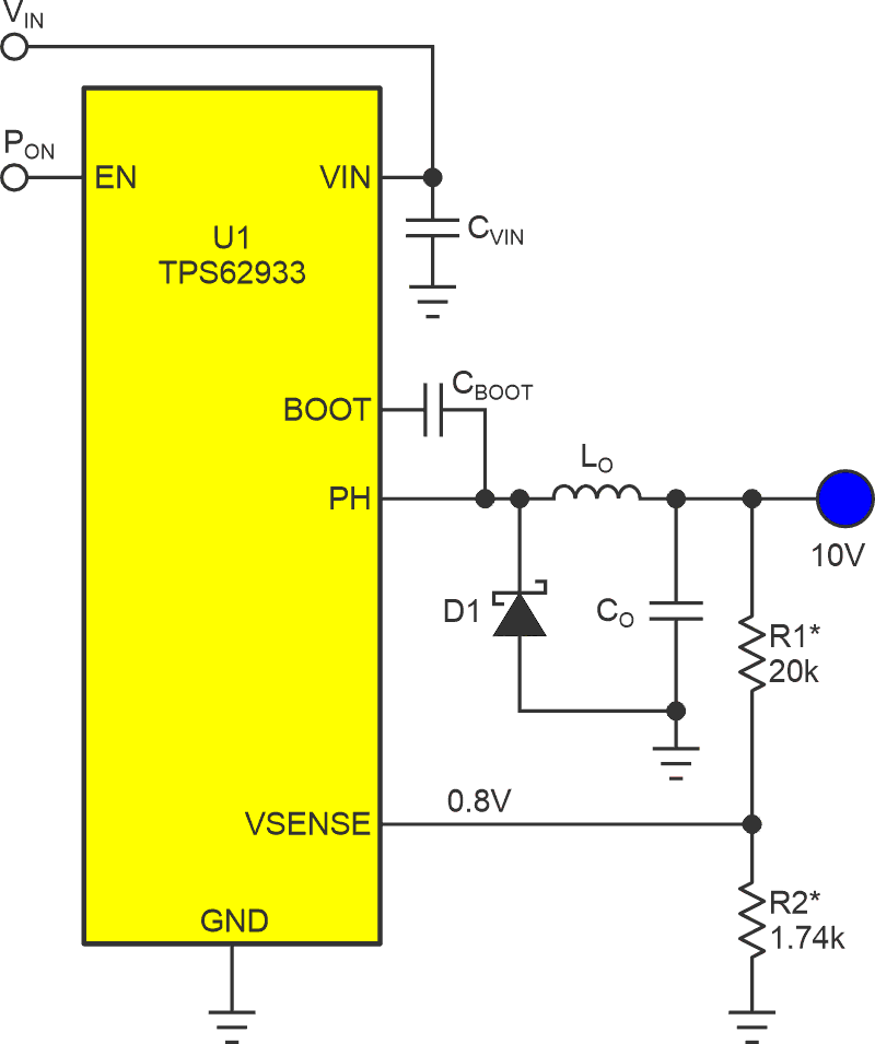
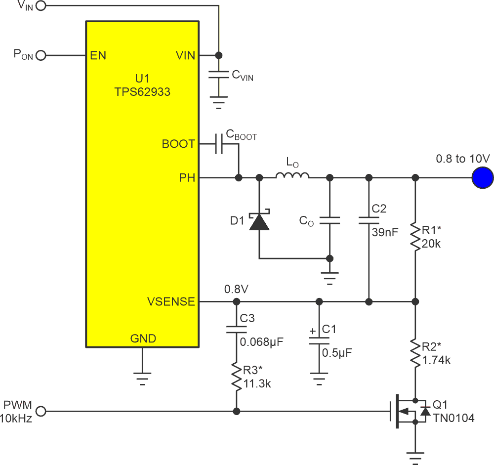
The three-component PWM-to-regulator solution
 |
|
| Figure 2. | Three parts comprise a circuit for linear regulator programming with PWM. |
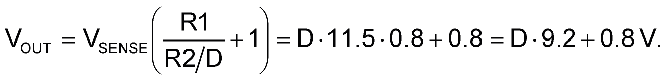
Figure 2 shows the simple three-component solution that the above topology makes possible. Note, the PWM duty factor (D) is from 0 to 1, where:
To introduce linear PWM control to the Figure 1 regulator, all that’s required is to add three discrete components: the PWM switch Q1, and the ripple filter capacitors C1 and C2. Note that VOUT will go to
for about 6 ms during power up while C1 and C2 are charging, but that should be okay.
The C2 capacitance required for 1 lsb (0.4%) PWM ripple attenuation is
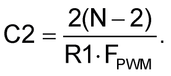
where N is number of PWM bits, and FPWM is the PWM frequency (10 kHz illustrated).
Then, to avoid messing with U1’s designed loop gain, possibly reducing stability,
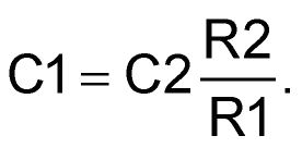
This capacitance ratio also provides protection for U1’s VSENSE input, since it ensures that even a sudden short of VOUT to ground can’t drive VSENSE dangerously negative.
This combination of time constants yields a first-order 8-bit settling time of T8 = R1C2ln(256) = 37 ms. More on this lengthy number shortly.
A cool feature of this simple topology is that, unlike many other schemes for digital power supply control, only the precision of R1, R2, and the regulator’s internal voltage reference matter for regulation accuracy. Precision is therefore independent of external voltage sources, e.g., logic rails. Precision, measured as percentage of VOUT, is also independent of D, and remains equal to VSENSE precision (e.g., ±1%) for all output voltages.
Speeding up the settling time
What if a 37-ms settling time is too lengthy for your application? What if you wouldn’t mind investing a couple more parts to speed it up? Figure 3 shows what.
First disclosed in EDN Design Idea (DI), “Cancel PWM DAC ripple with analog subtraction” (Ref. 1), a thrifty way to implement second-order PWM ripple filtering is through the analog subtraction of the AC component in the logic inverse of the PWM signal from the DC result. Figure 3 shows how that can be accomplished by simply adding R3 and C3 to the Figure 2 topology. Note that the impedance ratios of the added parts are equal to the ratio of the 5-Vpp PWM signal at Q1’s gate to the 0.8-Vpp logic complement at its drain = 5v/0.8v = 6.5. This is why R3 = 6.5×R2 and C3 = C2/6.5.
 |
|
| Figure 3. | Add R3 and C3 to get analog ripple subtraction (Ref. 1), second-order filtering, and a 7-ms settling time. The symbol “*” represents a precision of 1% or better. |
In closing: This DI revises an earlier submission, “Three discretes suffice to interface PWM to switching regulators” (Ref. 2).
References
- Woodward, Stephen. "Cancel PWM DAC ripple with analog subtraction."
- Woodward, Stephen. "Three discretes suffice to interface PWM to switching regulators."