Circuits for converting 4 to 20 mA analog current loop signals to 0 to 20 mA may be hot topics, but hot implementations of those circuits are not.
Circuit designs for conversion of 4 to 20 mA analog current loop signals, which are ubiquitous in process monitoring and control, to 0 to 20 mA are a hot topic recently. “Hot topic” is a perfect description because typical examples of such converters can dissipate half a Watt. Some cook even hotter than that! This results in some very un-green complications like TO220 packaged power pass transistors sporting substantial heatsinks. Would Greta T. approve? I think not!7
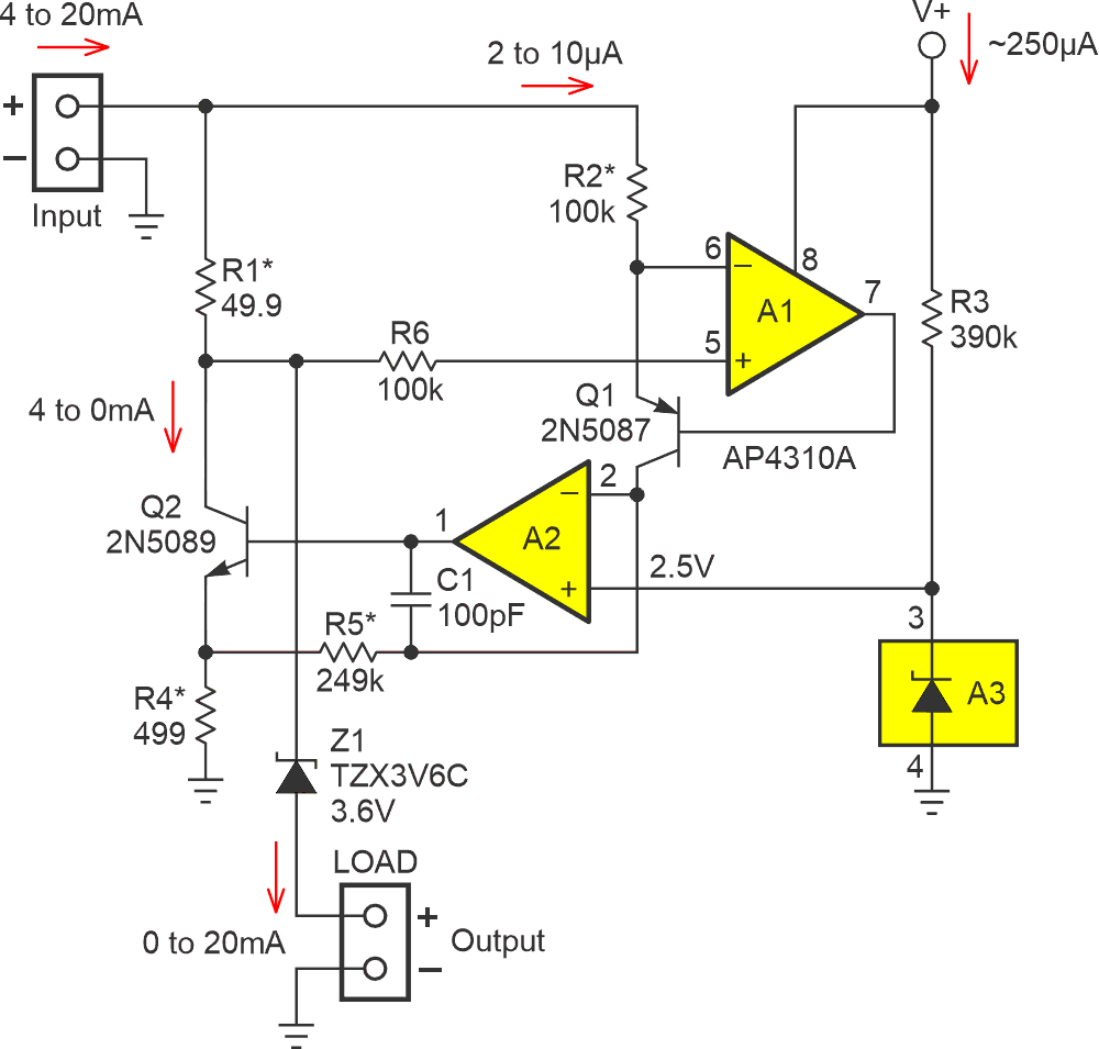
The design in Figure 1 offers a cool (and maybe even useful) efficiency improvement. It thriftily recycles most of the 4 to 20 mA input current to generate the 0 to 20 mA output while needing only microamps from its own local power supply. It consumes merely 250 µA × 24 V = 6 mW (typical) and dumps only similar single-digit milliwatts from Q2 (which is the closest thing it has to a pass transistor). That’s not even enough heat to make a TO92 tepid.
 |
|
| Figure 1. | This circuit’s operation is governed by the equation 1. The maximum current drawn from the local V+ supply is only 1/80th of max IOUT, translating to an 80:1 efficiency gain. Asterisked resistors are 0.5% precision or better. |
Here’s how it works.
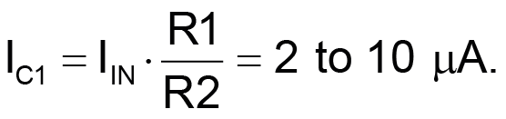
The 4 to 20 mA input current (99.95% of it, to be precise) passes through current sense resistor R1 and from there to the load, generating 200 mV to 1 V as IIN goes from 4 to 20 mA. The voltage to current converter R1+A1+Q1 makes that into
as the input to current to voltage converter R5+A2+Q2+R4, generating 0.5 to 2.5 V across R5. A2 compares this to A3’s 2.50 V internal reference, forcing Q2 to conduct so that the sum VR4 + VR5 = 2.5 V.
Thus
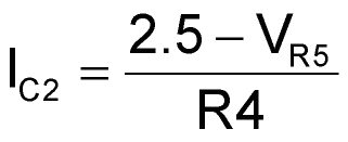
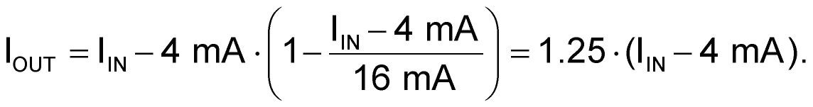
and it decreases linearly from 4mA to zero as IIN increases from 4 to 20 mA. The net effect is to force Q2 to subtract a linearly decreasing 4 to 0 mA from IIN, so that its 4 to 16 mA span is corrected to 0 to 20 mA in IOUT. In other (mathspeak) words:
 |
(1) |
The payoff is that 98.8% of IOUT comes from recycled IIN instead being sucked anew from V+.
V+ isn’t critical and needs only be sufficient to provide the compliance required by the (grounded) load. R3 needs to provide 50 µA bias for the A3pin3 shunt reference, so
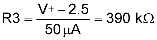
for V+ = 24 V. Noncritical Z1 provides a few volts of headroom for the transistors. The total voltage drop from input to output is 5.6 V.
Finally, there’s a caveat. In the event of complete loss of the nominal 4 to 20 mA input current, A2 will drive Q2 into saturation. This won’t damage anything, but will force A2 to draw 5 mA from V+ to supply the required Q2 base current.