IBM and Micron Technology announced that Micron will begin production of a new memory device built using the first commercial CMOS manufacturing technology to employ through-silicon vias (TSVs). IBM's advanced TSV chip-making process enables Micron's Hybrid Memory Cube (HMC) to achieve speeds 15 times faster than today's technology.
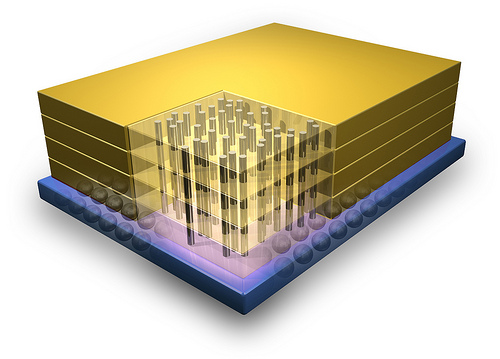
Micron's Hybrid Memory Cube features a stack of individual chips connected by vertical pipelines or “vias,” shown above. IBM’s new 3-D manufacturing technology, used to connect the 3D micro structure, will be the foundation for commercial production of the new memory cube.
HMC parts will be manufactured at IBM's advanced semiconductor fab in East Fishkill, N.Y., using the company's 32nm, high-K metal gate process technology.
HMC technology uses advanced TSVs — vertical conduits that electrically connect a stack of individual chips — to combine high-performance logic with Micron's state-of-the-art DRAM. HMC delivers bandwidth and efficiencies a leap beyond current device capabilities. HMC prototypes, for example, clock in with bandwidth of 128 gigabytes per second (GB/s). By comparison, current state-of-the-art devices deliver 12.8 GB/s. HMC also requires 70 percent less energy to transfer data while offering a small form factor — just 10 percent of the footprint of conventional memory.
HMC will enable a new generation of performance in applications ranging from large-scale networking and high-performance computing, to industrial automation and, eventually, consumer products.