Part 1
Preserved DC Precision
In a typical operational amplifier circuit, a portion of the output is fed back to the inverting input (Figure 9). Errors that are present on the output which were generated in the loop are multiplied by the feedback factor (β) and subtracted out. This helps maintain the fidelity of the output with respect to the input multiplied by the closed-loop gain (A).
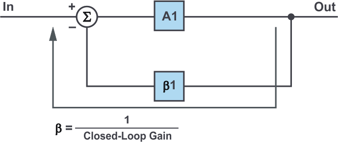 |
| Figure 9. |
Operational amplifier feedback loop. |
For the composite amplifier, amplifier A2 has its own feedback loop, but A2 and its feedback loop are all inside the larger feedback loop of A1 (Figure 10). The output now contains the larger errors due to A2 which are fed back to A1 and corrected. The larger correction signal results in the precision of A1 being preserved.
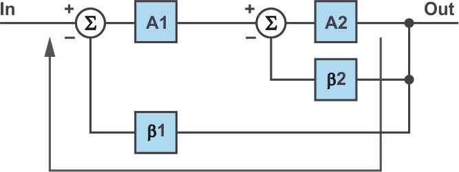 |
| Figure 10. |
Composite amplifier feedback loop. |
The effect of this composite feedback loop can be clearly seen in the circuit and results in Figure 11 and Figure 12. Figure 11 shows a composite amplifier comprised of two ideal op amps. The composite gain is 100 and the AMP2 gain is set to 5. VOS1 represents a 50 µV offset voltage for AMP1 while VOS2 represents a variable offset voltage for AMP2. Figure 12 shows that as VOS2 is swept from 0 mV to 100 mV, the output offset is not affected by the magnitude of error (offset) contributed by AMP2. Instead, the output offset is proportional only to the error of AMP1 (50 µV multiplied by the composite gain of 100) and remains at 5 mV regardless of the value of VOS2. Without the composite loop, we would expect the output error to increase as high as 500 mV.
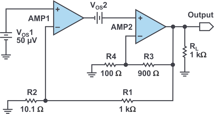 |
| Figure 11. |
Offset error contribution. |
| |
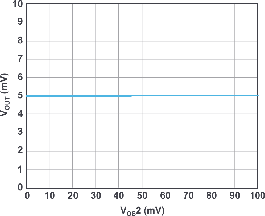 |
| Figure 12. |
Composite output offset vs. VOS2. |
| Table 2. |
Output Offset Voltage for Gain of 100 |
| Amplifier |
Effective VOS
(mV) |
VOS Reduction
(Composite Configuration) |
| AD8397 |
100 |
|
| AD8397 + ADA4091 |
3.5 |
28.6× |
| AD8397 + AD8676 |
1.2 |
83.3× |
| AD8397 + AD8599 |
1 |
100× |
|
Noise and Distortion
The output noise and harmonic distortion of the composite amplifier are corrected in a similar fashion as the dc errors, but, in the case of ac parameters, the bandwidth of the two stages also comes into play. We will look at an example using output noise to illustrate this with the understanding that distortion cancellation occurs in much the same manner.
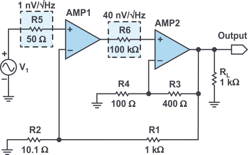
Referring to the example circuit in Figure 13, for as long as the first stage (AMP1) has enough bandwidth, it will correct for the larger noise of the second stage (AMP2). As AMP1 begins to run out of bandwidth, the noise from AMP2 will begin to dominate. However, if AMP1 has too much bandwidth, and peaking is present in the frequency response, a noise peak will be induced at the same frequency.
 |
| Figure 13. |
Noise sources of composite amplifier. |
For this example, resistors R5 and R6 in Figure 13 represent the inherent noise sources for AMP1 and AMP2 respectively. The top plot of Figure 14 shows the frequency response for various AMP1 bandwidths as well as that of AMP2 for a single fixed bandwidth. Recall from the section on gain-splitting that a composite gain of 100 (40 dB) and AMP2 gain of 5 (14 dB) will force an effective AMP1 gain of 20 (26 dB) as can be seen here.
 |
| Figure 14. |
Noise performance vs. stage 1 bandwidth. |
The bottom plot shows the wideband output noise density for each case. At low frequencies, the output noise density is dominated by AMP1 (1 nV/√Hz times the composite gain of 100 equals 100 nV/√Hz). This will continue for as long as AMP1 has enough bandwidth to compensate for AMP2.
For the cases where AMP1 has less bandwidth than AMP2, the noise density will begin to be dominated by AMP2 as AMP1 bandwidth begins to roll off. This can be seen in two of the traces of Figure 14 as the noise climbs to 200 nV/√Hz (40 nV/√Hz times the AMP2 gain of 5). Lastly, in the case where AMP1 has much greater bandwidth than AMP2, resulting in a peaking in the frequency response, the composite amplifier will exhibit a noise peak at the same frequency, also shown in Figure 14. Since the frequency response peaking results in excessive gain, the amplitude of the noise peak will also be higher.
Table 3 and Table 4 shows the effective noise reduction and the THD+n improvement when using various precision amplifiers as the first stage in a composite amplifier with the AD8397.
| Table 3. |
Noise Reduction Using Different Front-End Amplifiers
with Effective Gain = 100 at f = 1 kHz |
| Configuration |
Noise, en
(nV/√Hz) |
Effective Noise
Reduction (%) |
| AD8397 Only |
450 |
|
| AD8397 + ADA4084 |
390 |
13.33 |
| AD8397 + AD8676 |
280 |
37.78 |
| AD8397 + AD8599 |
107 |
76.22 |
|
| Table 4. |
THD+n Comparison Using Different Front-End Amplifiers
with Effective Gain = 10 at f = 1 kHz and ILOAD = 200 mA |
| Configuration |
Effective
THD+n (dB) |
THD+n Improvement
(dB) |
| AD8397 Only |
–100.22 |
|
| AD8397 + ADA4084 |
–105.32 |
5.10 |
| AD8397 + AD8676 |
–106.68 |
6.46 |
| AD8397 + AD8599 |
–106.21 |
5.99 |
|
System-Level Application
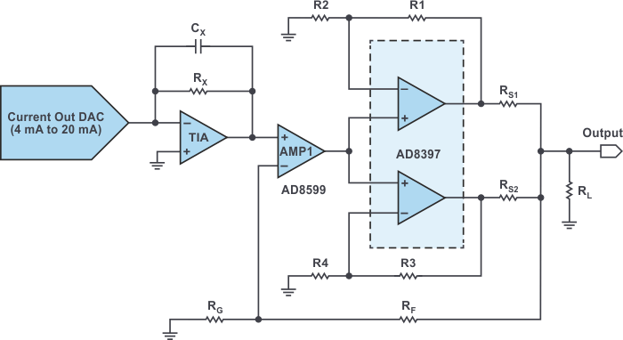 |
| Figure 15. |
Application circuit for DAC output driver. |
In this example (Figure 15), the goal for a DAC output buffer application is to provide an output of 10 V p-p into a low impedance probe with a current of 500 mA p-p, low noise and distortion, excellent dc precision, and as high of a bandwidth as possible. The output of a 4 mA to 20 mA current-out DAC is to be converted to a voltage by the TIA, then to the input of the composite amplifier for more amplification (Figure 16). With AD8397s on the output, the output requirements are attainable. AD8397 is a rail-to-rail, high output current amplifier capable of delivering the needed output current.
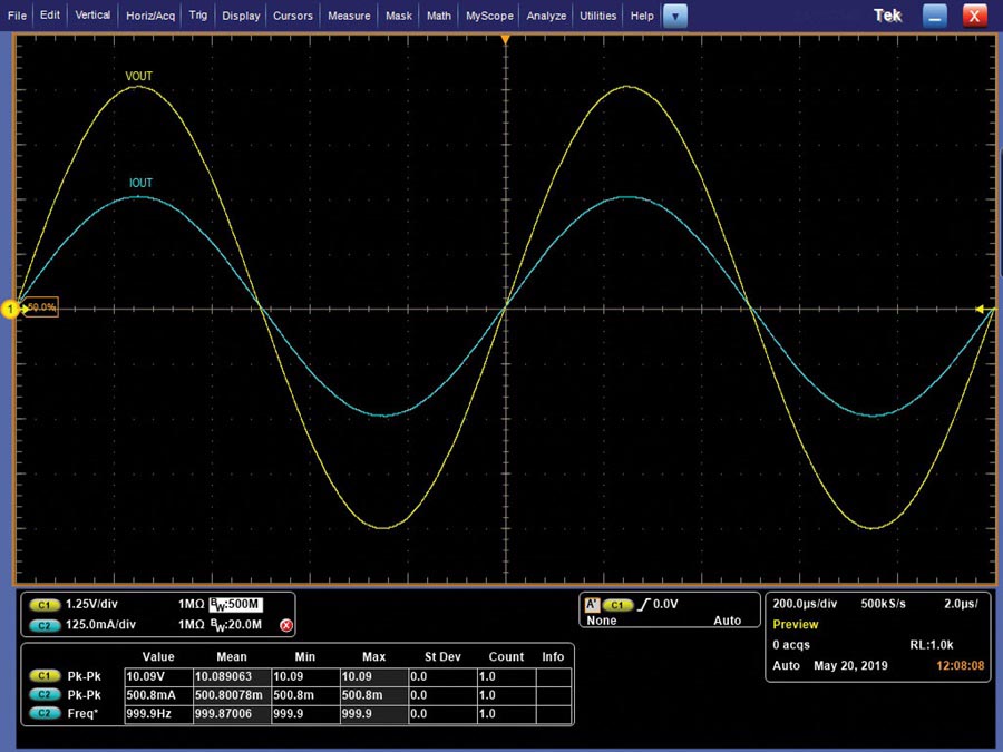 |
| Figure 16. |
VOUT and IOUT for AD8599 and AD8397 composite amplifier. |
AMP1 could be any precision amplifier that has the desired dc precision needed for the configuration requirement. In this application, various front-end precision amplifiers could be used with AD8397 (and other high output current amplifiers) to attain both the excellent dc requirements and the high output capability drive needed for the application (Table 5).
| Table 5. |
AD8599 + AD8397 Composite Amplifier
Specifications |
| Parameter |
Value |
| Gain |
10 V/V |
| –3 dB Bandwidth |
1.27 MHz |
| Output Voltage |
10 V p-p |
| Output Current |
500 mA p-p |
| Output Offset Voltage |
102.5 µV |
| Voltage Noise (f = 1 kHz) |
20.95 nV/√Hz |
| THD+n (f = 1 kHz) |
–106.14 dB |
|
This configuration is not limited to AD8397 and AD8599, but is possible with other combinations of amplifiers to cater this output drive specification that requires excellent dc precision. The amplifiers in Table 6 and Table 7 are also suited for this application.
| Table 6. |
Amplifiers with High Output Current Drive |
High Output Current
Amplifiers |
Current
Drive (A) |
Slew Rate |
VS Span,
Max (V) |
| ADA4870 |
1 |
2.5 kV/μs |
40 |
| LT6301 |
1.2 |
600 V/μs |
27 |
| LT1210 |
2 |
900 V/μs |
36 |
|
| Table 7. |
Precision Front-End Amplifiers |
| Precision Amplifiers |
VOS
(μV) |
VNOISE, en
(nV/√Hz) |
THD+n,
1 kHz (dB) |
| LT6018 |
50 |
1.2 |
–115 |
| ADA4625 |
80 |
3.3 |
–110 |
| ADA4084 |
100 |
3.9 |
–90 |
|
Conclusion
With the composite amplifier, the marriage of two amplifiers realizes the best specifications that each one offers while compensating for their limitations. Amplifiers with high output drive capability combined with precision front-end amplifiers could provide solutions to applications with challenging requirements. When designing, always consider stability, noise peaking, bandwidth, and slew rate for optimum performance. There are plenty of possible options to cater a wide range of applications. With the proper implementation and combination, striking the right balance for the application is highly achievable.
Materials on the topic
analog.com