Introduction
Modern portable electronic devices require a high-capacity Lithium-ion battery to power popular features such as high-definition cameras, edge-to-edge high-resolution touchscreens and high-speed data connections. As a result, charging power sources like USB Type-C® have increased their output power capabilities to support faster battery charging for high-capacity batteries.
Traditional synchronous buck-based battery chargers cannot take full advantage of high input power because of their maximum efficiency limitations. The challenge for portable electronics designers is how to fit a high-efficiency battery charging solution in a small footprint that fully utilizes high input power to achieve fast and cool charging.
A three-level converter topology that includes added capacitive storage elements and power switches can increase the equivalent switching frequency, fSW, and generate a lower voltage across the inductor, which enables the use of a smaller inductor. This improves total system efficiency, with lower power losses and cooler operating temperatures in a smaller footprint when compared to traditional synchronous buck converters. This article presents an analysis of the three-level buck topology and provides an operation and power-loss comparison between synchronous buck and three-level buck battery chargers, including variances in charging current between the three- and two-level buck topologies.
Traditional buck topology
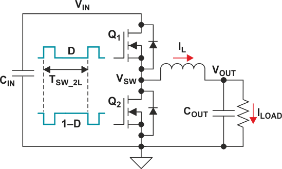
The synchronous two-level (2L), step-down (buck) switching topology has been around for decades. A traditional buck switching converter consists of two metaloxide silicon field-effect transistors (MOSFETs or FETs), one inductor, an input capacitor in parallel with the input source and an output capacitor, as shown in Figure 1.
 |
||
| Figure 1. | Two-level (2L) buck switches and gate drive. | |
The switch gate-drive signals are complementary, running at duty cycles D and 1 – D. The node between the switches, VSW, alternates between VIN and 0 V; hence the term “two-level converter.” When Q1 is on and Q2 is off, the inductor is charging and is providing current to the output. When Q2 is on and Q1 is off, the inductor discharges to provide current to the output. This produces a fixed duty-cycle square waveform that when filtered by the inductor and output capacitor provides an output voltage.
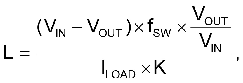
Assuming ideal FETs and continuous inductor current, the steady-state duty cycle is D = VOUT/VIN. The fSW determines the inductor’s inductance, based on V = L × di/dt and rearranged as Equation 1:
 |
(1) |
where K is the inductor current ripple as a percentage of output current, chosen to be 20% to 40%.
For battery charging applications with wide input-voltage ranges, existing semiconductor processes and inductor technology limit fSW to 1 to 2 MHz. Higher switching frequencies cause transistor switching losses and inductor second-order AC losses to dominate converter losses. Therefore, when trying to increase converter efficiency and reduce heat dissipation, the common solution is to increase inductor footprint size for a lower DC resistance (DCR).
Three-level buck operation
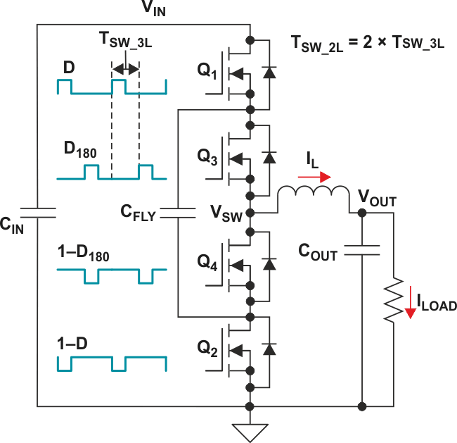
The three-level (3L) buck converter illustrated in Figure 2 is a combination of a switched flying capacitor, CFLY, and a switched inductor circuit, with two additional FETs, Q3 and Q4.
 |
||
| Figure 2. | Three-level (3L) buck switches and gate drive. | |
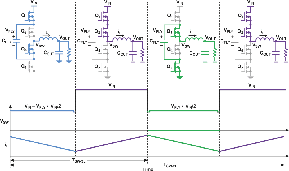
The gate-driving scheme is similar to that of a traditional two-phase buck converter. A complementary signal drives the outer FETs, Q1 and Q2, with duty cycle D = VOUT/VIN, just like the two-level (2L) buck converter. A second complementary signal of equal duty cycle drives the inner FETs, Q3 and Q4, but is phase-shifted from the outer FET’s signal by 180 degrees. By keeping CFLY balanced at VIN/2, the VSW switch node alternates between VIN, VIN/2 and ground; hence the term “three-level.”
 |
||
| Figure 3. | Three-level (3L) converter operation with D less than 0.5. | |
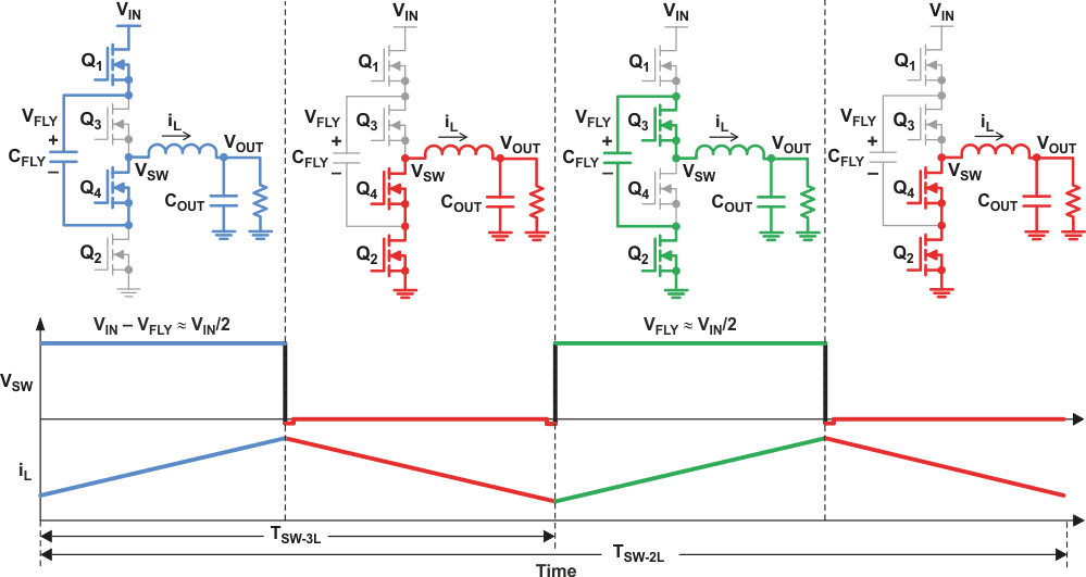
Figure 3 shows a complete switching cycle when the duty cycle is less than 0.5 (that is, when the input voltage is more than twice the output voltage). Figure 4 on the next page shows the complete switching cycle when the duty cycle is greater than 0.5.
 |
||
| Figure 4. | Three-level (3L) converter operation with D greater than 0.5. | |
At D = 0.5 (50%), Q1 and Q4 are on for half of the period; Q3 and Q2 are on for the other half. This results in VSW remaining at VIN/2, which by definition is equal to VOUT. There is no voltage across the inductor, so the ripple current goes to zero.
Because the FETs are driven 180° out of phase, the switching frequency, fSW-3L, at the VSW node is double that of a comparable 2L converter, fSW-2L. Each FET only turns on once during the 2L period, therefore TSW-2L = 2 × TSW-3L.
Three-level (3L) buck on-chip losses
Table 1 compares the 2L buck converter on-chip losses, PON-CHIP, to those in the 3L buck converter. On-chip losses include conduction losses from the switches’ resistances, PCOND; switching charge losses, POSS and PGATE; reverse recovery losses, PQRR; current-voltage losses during gate turn-on and turn-off, PIV; and loss across the body diodes during the dead time when both switches are off, PDT. Assuming CFLY is balanced at VIN/2, the 3L buck-converter FETs only need to block half the voltage as compared to the 2L buck converter FETs.
| Table 1. | Equations for comparing estimated power-loss | ||||||||||||||||||||||||||||
|
|||||||||||||||||||||||||||||
Making the above assumptions about the 2L and 3L losses enables a theoretical comparison of the on-chip power losses between the two topologies as shown in Table 1. The following bullets are highlights from this theoretical comparison:
- The fSW and inductor current ripple are the same for both topologies, which means that the 3L inductance value, L3L, is one-fourth that of the 2L, L2L. This is explained more thoroughly in the next section.
- The area allocated for the 2L high-side (HS) FET is equal to the sum of the area for the 3L HS FETs (i.e., AQ1-2L = AQ1-3L + AQ3-3L). With the 3L FETs at one-half the 2L FET’s voltage rating, the FET resistances are equal (i.e., RQ1-2L = RQ1-3L = RQ3-3L). The same applies to the low-side FETs. This results in the 3L total FET resistance being twice that of the 2L buck for a fixed area.
- If the 3L FETs are at one-half the voltage of the 2L FET but the 3L FETs are driven with the same transient voltages, dv/dt, at VSW, the turn-on and turn-off times are cut in half. This results in PIV being reduced by one-half.
- Using the same area, the total stored charge remains the same, meaning QOSS(Q1)-2L = QOSS(Q1)-3L + QOSS(Q3)-3L and it is the same for QOSS(Q2)-2L. The total stored charge is actually less because the 3L FETs are at one-half the voltage, but this can be ignored in a simple analysis.
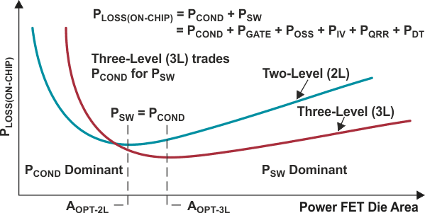
As shown in the far-right column of Table 1, for the same die area, the 3L topology conduction and dead-time losses double. But because the 3L FETs see one-half the input voltage compared to the 2L buck, POSS and PIV losses are halved. An increase in FET area makes it possible to lower conduction losses until switching losses begin to dominate, as shown in Figure 5.
 |
||
| Figure 5. | On-chip losses vs. die area. | |
The optimal FET areas, AOPT-2L and AOPT-3L, occur where switching losses equal conduction losses.