Three-level (3L) buck off-chip components and their losses
Off-chip losses include those across the equivalent series resistance (ESR) in the input, output and flying capacitors, as well as the inductor. Choosing ceramic capacitors with very low (<20 mΩ) ESR renders their losses almost negligible. Input and output capacitors for the 3L converter are also sized based on acceptable input ripple current and output voltage ripple, just as they are for a 2L converter.
 |
||
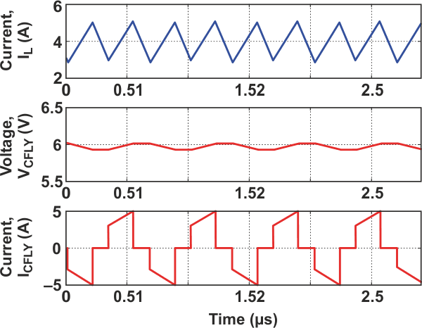
| Figure 6. | CFLY ripple voltage and current relative to inductor ripple current. | |
Sizing CFLY for acceptable ripple voltage and current is critical for 3L operation. In fact, keeping CFLY balanced at VIN/2 during transients, startup, at light load and D = 100% is not trivial and requires some additional, proprietary circuitry not shown in Figure 2. Figure 6 shows an example waveform for ∆IFLY relative to normalized ∆IL.
Equations 2 and 3 are for CFLY ripple voltage and current:
 |
(2) |
 |
(3) |
CFLY ripple voltage peaks at D = 0.5 and increases directly with load current. After factoring in ceramic capacitor derating from DC bias and temperature, CFLY must withstand half the input voltage. Note that at D = 0.5, IC(FLY) sees the full load current. CFLY capacitance is sized to keep DVC(FLY) less than 10% of VIN/2 in order to ensure loop stability. To ensure long capacitor life, the capacitor package size and RMS current rating must be large enough to handle the associated temperature rise.
Inductor losses consist of DCR losses, PDCR, and core losses, PCORE. The DCR losses increase with inductance value, which is a function of fSW.
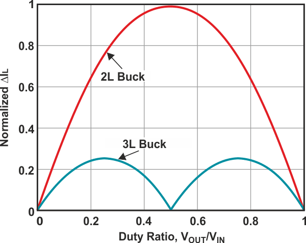
The 180-degree phase-shifted gate drive for Q3 and Q4 effectively doubles the converter’s switching frequency at VSW. Additionally, by keeping CFLY balanced at VIN/2, the three-level converter reduces the volt-seconds across the inductor by half. The combination results in a one-quarter reduction in inductor ripple given the same inductor and fSW. The reduction in inductor ripple current compared to the 2L converter switching at the same frequency over duty cycle is apparent in Figure 7.
 |
||
| Figure 7. | Duty cycle comparison of 2L and 3L converters. | |
In a 3L converter, Equation 4 derives the inductance value:
 |
(4) |
and Equation 5 calculates the inductor DCR losses:
 |
(5) |
Equation 5 confirms that inductor current ripple has little effect on PDCR. Like the 2L buck converter, the 3L converter requires an inductor with lower DCR for higher efficiency. As explained above, the topology inherently provides a one-quarter reduction in inductor ripple current. If the application can accept the inductor ripple current and resulting output voltage ripple from a comparable 2L converter operating at the same switching frequency, an inductor with one-quarter the inductance value could be used, which is available in a package with a much smaller footprint.
Assuming that inductor DCR scales proportionally with the inductance value, the inductor losses for the 3L converter, PDCR-3L, are one-fourth that of the 2L converter, PDCR-2L/4. The smaller package yields a smaller total solution size, while the lower DCR yields higher efficiency. Therefore, for the same thermal budget, these benefits enable the 3L converter to provide a higher output current in a smaller area (that is, a higher power density) compared to a 2L buck solution.
Comparing 3L and 2L buck charging solutions
TI’s latest 3L, single-cell buck charger, the BQ25910, operates at fSW = 750 kHz and is capable of providing 5 A of battery charge current. Comparatively, TI’s BQ25898 4-A 2L charger comes in a similar chip-scale package, with an older silicon process technology, but operates at an fSW = 1.5 MHz. The BQ25898 uses a 1-μH inductor while the BQ25910 uses a 470-nH inductor—which is only one-half and not the potential one-fourth reduction in inductance that the 3L topology enables.
Table 2 compares component areas for the two chargers, using inductors with similar current ratings and reasonable DCR. The table also excludes routing and ignores common components for both chargers such as the input capacitor, PMID-pin capacitor and linear-regulator capacitor.
| Table 2. | Component area comparison | ||||||||||||||||||||||||||||||
|
|||||||||||||||||||||||||||||||
Even with the additional capacitors, the BQ25910’s smaller footprint but similar DCR inductor and lack of battery FET results in a 36% reduction in printed circuitboard (PCB) area.
Figure 8 shows the power losses for the BQ25910, modeled using the equations in Table 1 and actual silicon process data. Also shown are the losses for the BQ25898. Note how the inductor DCR losses dominate the total losses for both chargers.
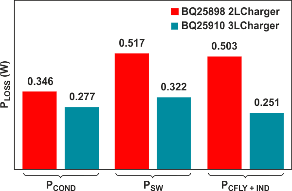 |
||
| Figure 8. | modeled power losses. | |
Figure 9a shows a plot of the BQ25910 and BQ25898 measured efficiency at a 9-V input voltage and a 3.8-V battery voltage. Figure 9b compares the losses of the two converters. At a 3-A charge current, the BQ25898 efficiency is 89.3%. From Figure 8, the BQ25910’s PLOSS is 0.850 W from a total output power of 3 A × 3.8 V = 11.4 W, resulting in 93.1% efficiency, which is very close to the measured 93.2%.
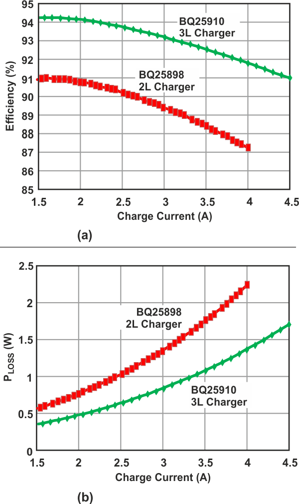 |
||
| Figure 9. | BQ25910 and BQ25898 measured efficiency and power losses. | |
At a 9-V input voltage, 3.8-V battery voltage and 3-A charge current, the 3L BQ25910 has a 3.9% efficiency improvement and 36% loss reduction. For a loss budget of 1.5 W, the BQ25898 can provide 3.2 A of charge current, while the BQ25910 can provide 4.2 A of charge current (a 31% increase) in a 36% smaller solution size.
Conclusion
Consumers want their personal electronics, with their ever-increasing battery capacity, to charge as quickly as possible. Achieving more than 90% efficiency for 3-A and higher charging currents from a 9-V or higher adapter in a small footprint remains difficult with traditional 2L buck switching chargers. Battery charging solutions are needed that fit in the smallest footprint while providing the optimal charging current, not only for improved battery safety and lifetime, but also for acceptable charging time and device temperature. The 3L buck switching chargers offer improved efficiency while reducing total solution size for compact design requirements.