Many applications call for wide-range-tunable LC oscillators that can deliver a nearly constant-frequency, nearly harmonic-free output even when the circuit's output load changes. From a design viewpoint, eliminating either inductive or capacitive LC circuit taps and transformer couplings within the frequency-determining circuit simplifies fabrication and production, as does the option of grounding one side of the tuned LC circuit. These requirements suggest a circuit that can automatically and efficiently internally adjust loop gain, the basic criterion for oscillation. In addition, the circuit must provide sufficient gain to oscillate with low-impedance LC circuits and regulate the oscillation's amplitude to improve frequency stability and minimize THD (total harmonic distortion).
 |
|
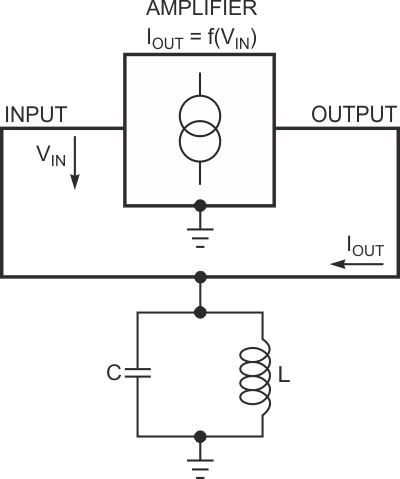
| Figure 1. | A parallel LC circuit and an amplifying voltage-to-current converter form a basic oscillator. |
Designers have exploited many circuit topologies – some highly complex – in their attempts to achieve these design goals, but certain active devices' basic properties can help designers obtain acceptable behavior from a simple oscillator circuit. Figure 1 shows a basic LC-oscillator arrangement. The amplifier operates as a noninverting voltage-controlled current source. The LC circuit converts the amplifier's output current, IOUT, to voltage, VIN, and applies it as input to the amplifier. Equation 1 shows the formal condition for oscillation:
 |
(1) |
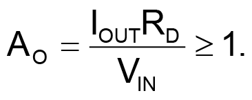
In this equation, AO is the overall voltage amplification and RD is the LC circuit's dynamic resistance at its resonant frequency. In practical circuits, the value of RD depends on the LC circuit's properties and thus can fall anywhere within a wide range. Also, Equation 1 assumes an ideal amplifier – that is, one having characteristics that are independent of frequency.
Figure 1 and Equation 1 yield a simple insight into the basic design problem: If the operation over a wide frequency range demands the use of several LC circuits with widely varying values of RD, the amplifier's properties must be adjustable over a wide range. You can adjust the amplification to fulfill the gain-limitation condition for the worst-case LC circuit and then rely on device nonlinearities to reduce amplification under overdrive conditions. However, a heavily overdriven amplifier's input- and output-differential resistances can drop to a fraction of their optimum, high-resistance values. Second, large amounts of nonlinear distortion can impair frequency stability. Moreover, these effects depend heavily on the amplifier's power-supply voltage, causing frequency stability to deteriorate if the supply voltage varies with load.
 |
|
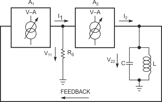
| Figure 2. | Adding a second voltage-to-current converter isolates the tuned circuit. |
Various oscillator circuits use different designs within the amplifier block in Figure 1. The popular common-emitter or common-source transistor stage presents two important drawbacks: First, it's an inverting amplifier, and, second, its output does not behave as a good current source, especially when heavily overdriven. Attempts to avoid these problems include transformer coupling or providing impedance-matching taps on the LC circuit, both of which complicate the design and only partially solve the problems.
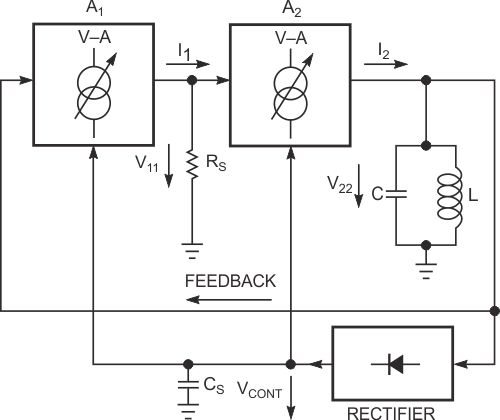
As Figure 2 shows, another oscillator topology features two cascaded noninverting amplifiers, A1 and A2, as voltage-to-current converters (voltage-controlled current sources). In the circuit, coupling resistor RS converts amplifier A1’s output current, IIN, to voltage VIN, and drives the second stage, A2. The tuned circuit's dynamic resistance converts A2’s output current to output voltage, V22, which feeds back to A1’s input to complete the positive-feedback loop. The overall loop amplification, ATOTAL, appears in Equation 2:
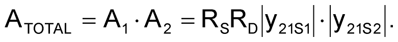 |
(2) |
In this equation, RD = QωL is the dynamic resistance of the LC circuit at resonance at the ω frequency, Q is the quality factor of the LC circuit, A1 and A2 are the equivalent voltage amplifications of both amplifier stages, and |y21S1| and |y21S2| are the real parts of differential-forward-transfer admittances of both amplifying stages. For self-sustained oscillations, the basic condition ATOTAL > 1 in Equation 1 must apply for all values of the LC circuit's dynamic resistance, RD. In theory, this condition presents no problem; however, in practice, a situation arises in which the circuit must operate as an LC oscillator with a broad range of tuning inductances and capacitances; a wide range of tuned-circuit quality-factor Q, which the inductor primarily determines; a constant-amplitude output at any combination of conditions A and B; and the best possible frequency stability versus supply voltage and load.
 |
|
| Figure 3. | Rectifying a portion of the signal provides a gain-control voltage for the amplifiers. |
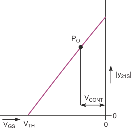
Most LC oscillator circuits cannot simultaneously fulfill all of these requirements. Some oscillator circuits can sequentially fulfill some requirements, but none can fulfill all of them without complicating the circuit beyond reasonable limits. Figure 3 shows a circuit deriving an external dc control signal from V22 to control the voltage-to-current-conversion coefficients – that is, amplification factors – of A1 and A2. Applying amplification control to both stages considerably increases the control's effectiveness. In addition to the original positive feedback for starting and sustaining oscillation, you can add an indirect negative-feedback path to the oscillator circuit to limit V22’s amplitude. To meet the original design goals, amplifier blocks A1 and A2 should exhibit voltage-controlled input-versus-output characteristics, should possess linear-control amplification characteristics (Figure 4), should not invert the signal's phase, and should draw nearly no input current. Also, to emulate a current source, A2 should present the highest possible differential internal output resistance.
 |
|
| Figure 4. | Control characteristics of an idealized JFET exhibit linear variation of forward transconductance versus gate-to-source voltage. |
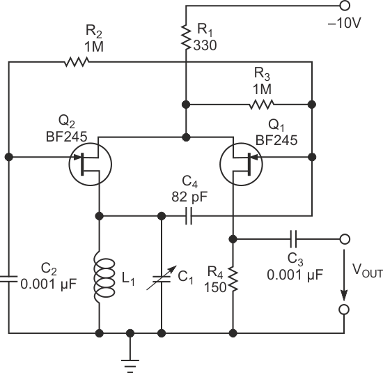
The best active devices for both amplifier stages are the selected N-channel, medium-grade BF245Bs JFETs with a drain current of 5 mA at a gate-to-source voltage of 0 V and a drain-to-source voltage of 15 V. Figure 5 shows the final circuit, in which Q2 operates as a common-drain amplifier, A2, and Q1 operates as a common-gate amplifier, A1.
 |
|
| Figure 5. | The completed oscillator circuit features a minimal component count. |
The gate-source junction of Q1 rectifies the ac voltage, V22, across the tuned circuit. Coupling capacitor C4 in Figure 5 doubles as dc-voltage-smoothing capacitor CS in Figure 3 because its bottom electrode connects to ground through the low dc resistance of tuning coil L. The dc-control voltage drives the gate of Q2 through resistor R2. Capacitor C2 connects Q2’s gate to ground for ac signals, and Q2 operates in common-gate connection because Q1’s source drives Q2’s source. To minimize frequency variations due to changing loads, a relatively low-value resistor, R4, in series with Q1’s drain, isolates the output from the circuit's frequency-determining components. In addition, one lead each of L and C connects to ground.
 |
|
 |
|
 |
|
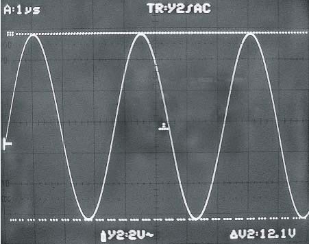
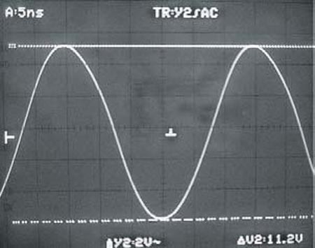
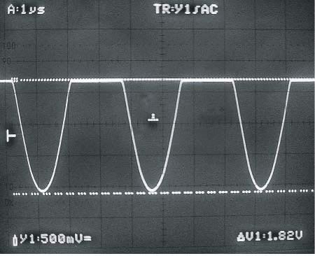
| Figure 6. | A clean sine wave (V22 in Figure 3) appears across the tuned circuit at 280 kHz for values of 147 µH and 2200 pF for L1 and C1, respectively (a). The sine wave with respective values of 56 µH and 60 pF differ (b). The output waveform at 280 kHz, for values of 147 µH for L1 and 2200 pF for C1, exhibits a flat top (c). |
The waveforms in Figure 6a and 6b show no substantial change in the voltage across the tuned circuit even for widely different values of L and C. The voltage across the tuned circuit remains constant within 3% over a supply-voltage range of 8 to 30 V. The same or better amplitude stability holds for the output voltage (Figure 6c), even at frequencies as low as 5 kHz and as high as 50 MHz with no adjustment of any passive-component values, except for L and C. Reducing the value of R4 yields a smaller output voltage, further diminishing the effects of load variations on the operating frequency.
The dc level of the top, flat part of VOUT rests at ground potential, and the waveform goes negative due to the negative power-supply voltage. Because of automatic-gain-control action, the waveshape remains remarkably consistent, regardless of frequency, exhibiting slightly rounded corners, mostly due to stray capacitances, at frequencies higher than 25 MHz. Only the LC circuit's ungrounded end provides a perfect sine wave. Other voltage and current waveforms exhibit cutoff distortion because both transistors operate roughly in Class B mode, shifting toward Class C at increasing power-supply voltages. You can extract a sine wave directly from the LC circuit, but variations in load impedance will influence the operating frequency.
On the other hand, the negative dc feedback controlling the gain of both transistors prevents even relatively large-load-impedance variations across the tuned circuit from greatly affecting the generated amplitude until the LC circuit's Q factor drops very low. At the expense of added complexity and a larger component count, you can include a buffer stage and extract a true sine wave from the LC circuit, but, in the circuit's original application as a radar-marker generator, the constant output amplitude ranked as of greater importance than the waveshape.