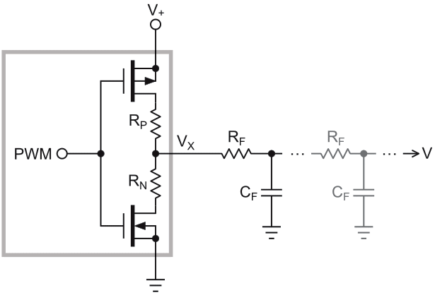
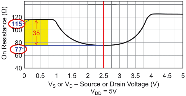
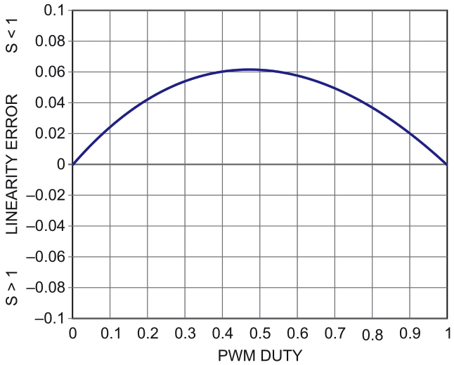
Simplicity and low cost sustain the popularity of passive PWM DAC ripple filters despite their limitations. One of these limitations is a high output impedance caused by the series sum of filter resistance(s) (RF in Figure 1, one resistor for each cascaded filter RC stage), making overall DAC accuracy very sensitive to output loading. The designers’ recourse, unless they want to resort to active output buffering and thus lose some of that wonderful PWM simplicity and cheapness, is to make RF as low as practical.
 |
|
| Figure 1. | A generic passive PWM filter topology with one resistor (RF) for each cascaded filter RC stage. |
So, how low is practical and what factors set the limit?
Although a ripple filter may comprise multiple stages, the first stage will generally take center stage in the “how low to go” decision, for these reasons:
In virtually all (even in multi-stage) ripple filter designs, RF of later stages (if any) are proportional to the first stage’s RF. So, when it’s known, they, and therefore the final DAC output impedance, are also known.
To a good approximation, the full peak-to-peak V+ PWM waveform amplitude usually appears across the first stage RF, so that practicality-limiting factors like power and current draw are almost entirely determined by its resistance. Worst case average power and current draw typically occur at or near 50% PWM duty cycle and are given by:
where RN is the N-channel switch’s on-resistance and RP is the P-channel switch’s on-resistance.
Suppose we choose 10 mW for maximum filter power dissipation and V+ = 2.5 V. Then filter output impedance is given by:
This 156 Ω would be a usefully low and loading-resistant output impedance (capable of holding 8-bit accuracy against 40k load resistance) and is actually similar to that of rail-to-rail buffer op amps when in zero-voltage output saturation. For comparison, consider a representative RRIO op amp (the TLV237x) whose guaranteed minimum output V when sinking 1 mA is 150 mV which converts to an equivalent impedance of:
See Low-level output voltage on page 8: https://www.ti.com/lit/ds/symlink/tlv2374-q1.pdf.
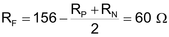
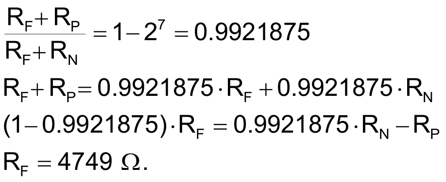
When Z = 156 Ω, the ripple filter is almost as good as a buffered output in some circuit states. This is surprising performance for a simple and cheap passive filter. But is it ultimately practical? The arithmetic above implicitly assumes RN = RP. What happens if they’re not, as shown in Figure 2’s on resistance (RON) versus source or drain voltage (V) graph for the sort of switch (TMUX4053) that might be used to generate a precision 2.5 V PWM waveshape?
 |
|
| Figure 2. | On-resistance versus source or drain voltage for the TMUX4053 with an unequal at |
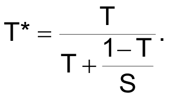
At 25 °C RP is 77 Ω and RN is 115 Ω. If we make:
now the net resistance that charges the filter capacitor:
= RF + RP = 60 + 77 = 137 Ω
is significantly smaller than the resistance that discharges it:
= RF + RN = 60 + 115 = 175 Ω
by a symmetry factor of:
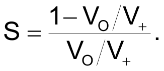
Unfortunately, while okay for minimizing output impedance, this much up/down resistance asymmetry is a bad thing for DAC integral linearity. Figure 3 shows the effect of S = 0.78 on linearity: A deal-breaking >6% of full-scale deviation from accurate linearity.
In fact, this is a general result. For any given S, integral nonlinearity of approximately:
can be expected, with deviation from linear going positive for S < 1 and negative for S > 1.
 |
|
| Figure 3. | Linearity error versus PWM duty where S = 0.78 creates ~6% of integral nonlinearity. |
Therefore, if we want abs(INL) = 29 for honest ½ LSB 8-bit linearity, we need:
abs(1 – S) = 4 × 29 = 27
and for the example considered:
Thus, the output impedance must increase by 30-fold to 4.8 kΩ to restore 8-bit linearity, making minimum loading for 8-bit accuracy ~1.2M. Yikes!
But perhaps there’s a simple and cheap solution to even this badly bent linearity problem?
Actually, there is. It consists of a straightforward arithmetic correction:
Let VO = desired DAC output. Then, instead of setting PWM duty to T = VO/V+ per usual practice, substitute T* from
Then integral linearity will be restored, provided that the value provided for S is accurate. Unfortunately, simply calculating S from typical RN and RP numbers taken from the switch datasheet will probably not be accurate enough. It would be preferable (maybe mandatory) to directly measure S for the actual devices used. But how can you measure RN and RP in an assembled circuit?
This easy in-circuit method will work with no need to bother trying to measure internal switch resistances:
- Set PWM duty factor = 0.5 = 50%
- Read VO and V+ with a high impedance voltmeter.
- Then S can be calculated as
Therefore, with this one-time voltage measurement and simple software-based correction, the minimal output impedance calculated above is compatible with 8-bit DAC linearity and is ultimately practical, after all.
Moral: Yes, you really can go that low, no op amp required.