Thanks to its internal hysteresis, the highly useful Schmitt-trigger circuit accepts a low-slew-rate input signal and produces a clean, glitch-free output transition. Unfortunately, user-programmable logic devices, such as CPLDs and FPGAs, generally offer no direct method of synthesizing Schmitt-trigger gates and buffers. This Design Idea shows how a few external components and some VHDL code can implement a Schmitt trigger and put it to work in several useful applications.
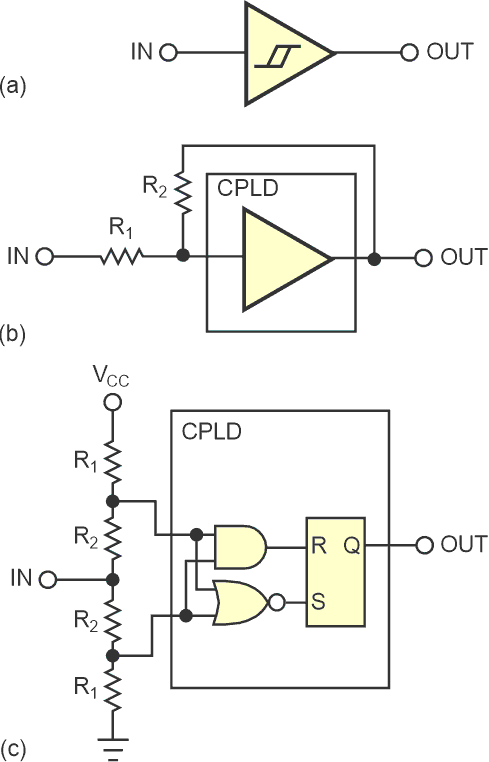
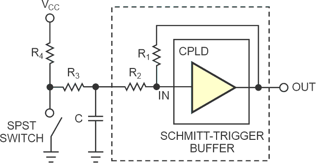
To create an equivalent of the basic Schmitt-trigger buffer, you use two external resistors to create positive feedback around a buffer (Figure 1a and b). You can also use four external resistors to set two threshold levels around an R-S flip-flop (Figure 1c).
 |
|
| Figure 1. | Use a portion of a programmable-logic device or gate array to implement a Schmitt-trigger buffer (a) by adding either two (b) or four external resistors (c). |
The following equations, respectively, describe the basic Schmitt trigger's positive- and negative-threshold levels:
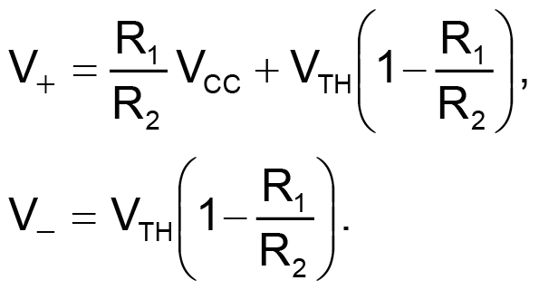
In these equations, VTH represents the input-voltage threshold of the CPLD/FPGA device, and VCC is its power-supply voltage.
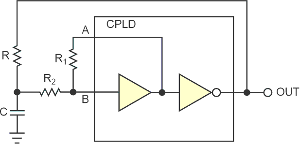
Based on the equivalent Schmitt-trigger circuit in Figure 1b, the low-cost resistance-capacitance oscillator in Figure 2 requires four external passive components. Resistor R and capacitor C set the circuit's oscillation frequency. Note that the resistance values of R1 and R2 must be larger than that of R. Listings 1 and 2 contain the circuit's VHDL implementation and RTL architecture, respectively.
Listing 1.
Entity Oscillator is
Port (
A : in std_logic;
B : in std_logic;
OUT : out std_logic
;)
end Oscillator;
Listing 2.
architecture RTL of Oscillator is
begin
A <= B;
OUT <= not A;
end RTL;
 |
|
| Figure 2. | Add a resistor and capacitor to a basic Schmitt-trigger buffer to form a low-cost oscillator. |
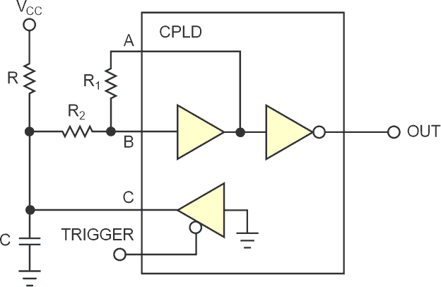
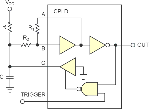
In Figure 3, an open-collector buffer provides the trigger for the basic Schmitt-trigger-retriggerable monostable circuit by discharging timing capacitor C. The circuit's output pulse width approximately equals the time constant RC. Listing 3 shows the VHDL implementation and RTL architecture, respectively.
Listing 3.
Entity Monostable is
Port (
A : in std_logic;
B : in std_logic;
Trigger : in std_logic;
C : out std_logic;
OUT : out std_logic
;)
end Monostable;
architecture RTL of Monostable is
begin
A <= B;
OUT <= not A;
C <= ’0’ when Trigger= ’1’ else ’Z’;
end RTL;
 |
|
| Figure 3. | An active-low buffer holds timing capacitor C discharged in this version of a retriggerable monostable multivibrator based on the Schmitt-trigger buffer. |
You can convert the retriggerable monostable into the nonretriggerable monostable in Figure 4 by using an open-collector NAND gate to discharge timing capacitor C. As long as the circuit's output remains high during the timing interval, the system locks out external triggers. As in the previous circuit, the output pulse width approximately equals the time constant RC. Listing 4 contains the VHDL and RTL codes.
Listing 4.
Port (
A : in std_logic;
B : in std_logic;
Trigger : in std_logic;
C : out std_logic;
OUT : out std_logic
;)
end Monostable;
architecture RTL of Monostable is
begin
A <= B;
OUT <= not A;
C <= ’0’ when Trigger= ’1’ and A=’0’ else ’Z’;
end RTL;
 |
|
| Figure 4. | A NAND gate locks out trigger pulses, forming a nonretriggerable, monostable circuit. |
You can use the basic CPLD buffer-with-feedback circuit to provide hysteresis for a contact-debouncing circuit. In Figure 5, resistor R4 provides contact-cleaning current, and R3 and C form a lowpass filter to reduce noise that contact bounce generates. Component values vary depending on the application.
 |
|
| Figure 5. | Use a Schmitt trigger to debounce switch contacts. |