I once needed a voltage doubler circuit with no DC leakage path between input and output, and ended up devising this unusual 556- (dual 555 timer) based circuit with a "floating" voltage output.
Despite some shortcomings, the 555/6 are remarkably versatile chips. Here, I take advantage of the high-current output drivers (>200 mA) in what could be called a push-pull configuration.
 |
||
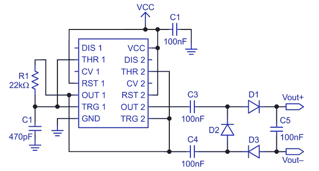
| Figure 1. | The pseudo-floating charge-pump voltage doubler. | |
The left half of U1 is connected so as to generate a 50% duty-cycle output. OUT1 drives one leg of the charge-pump, but also feeds the right half of U1, which is connected to simply invert its input. OUT2 drives the other leg of the charge-pump, 180° out of phase from OUT1.
The resulting square wave across D2 has an amplitude of 2·VCC, which D1, D3, and C5 convert to a DC output.
The output isn't truly floating, in that AC current could flow from input to output if they are at related potentials. However, there is no DC path from input to output, something I absolutely needed in the overall design, a DC solid-state relay.
Component values will depend on the required output current and the switching frequency. To minimize losses, diodes could be Schottky.