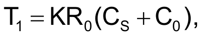
In some applications of capacitive sensors, the instrument’s front end must be small enough to fit into a narrow space. Figure 1 shows a precision capacitive-sensor interface for such use. The square-wave output from a low-voltage 555 timer, IC1, constantly triggers the precision one-shot, IC2, to produce quasistable outputs for time periods T1 and T2, which are proportional to external timing capacitance:
and
where K is the multiplier factor. K is nearly independent of the external timing capacitance when that capacitance is more than 100 pF. So, a 150 pF capacitor, C0, in shunt with the capacitive sensor, CS, supplies an offset so that operation of the one-shot remains within a linear range even if the value of CS is less than 100 pF.
 |
|
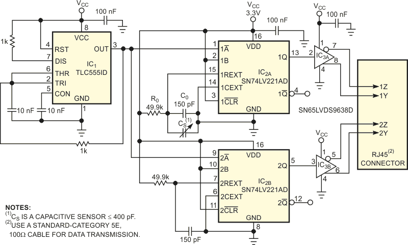
| Figure 1. | This compact capacitive-sensor-interface-circuit design permits great flexibility; you can easily integrate it into a miniature sensor head near the measurement point. |
To achieve good measurement accuracy, connect a reference channel with a fixed 150-pF capacitor. This method cancels the effects of both stray capacitance and transition time. A single 3.3 V supply powers this interface circuit. The circuit’s compact design permits flexibility, and you can easily integrate the circuit into a miniature sensor head near the measuring point. IC3 converts the outputs to LVDS (low-voltage-differential-signaling) levels and then transmits these outputs using a standard Category 5e cable to the terminal, which may be some distance away. As long as the cable is shorter than 10 m, the transmission bandwidth is adequate for ensuring acceptable measurement accuracy within several picofarads to hundreds of picofarads (Reference 1). In Figure 2, the terminal at IC4 converts the signals it receives from the interface to LVTTL (low-voltage-transistor-to-transistor-logic) levels and then feeds them to a set of passive filters. Each dc output is proportional to the signal’s duty cycle:

and
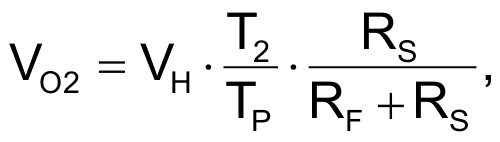
where VH is the high-level output voltage of IC4 and TP is IC1’s oscillation period. By digitizing the two outputs, you can obtain a reading proportional to the sensor’s capacitance, VO1 – VO2.
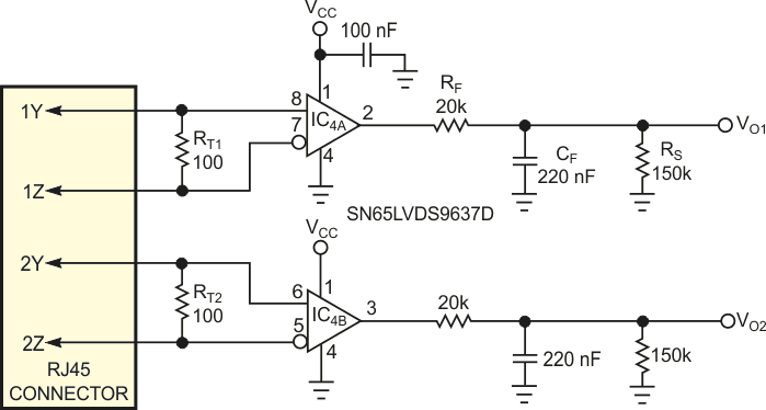 |
|
| Figure 2. | At the terminal, IC4 converts the signals it receives from the interface to LVTTL levels and then feeds them to a set of passive filters |
Be sure that T1 < P, – that is,
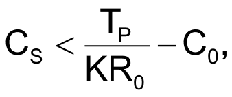
otherwise, the final output will be erroneous. For the sake of a wide measurement range, keep TP as long as the target application permits.