Integrating ADCs that provide accurate results without requiring a precision integrator capacitor has been around for a long time. A venerable example is that multimeter favorite, the dual-slope ADC. That classic topology uses just one integrator to alternately accumulate both incoming signal and complementary voltage references with the same RC time constant. It thus automatically ratios out time constant tolerance. Slick.
This Design Idea (DI) will describe a (possibly) new integrating converter that reaches a similar goal of accurate conversions without needing an accurate capacitor. But it gets there via a significantly different route. Along the route, it picks up some advantageous wrinkles.
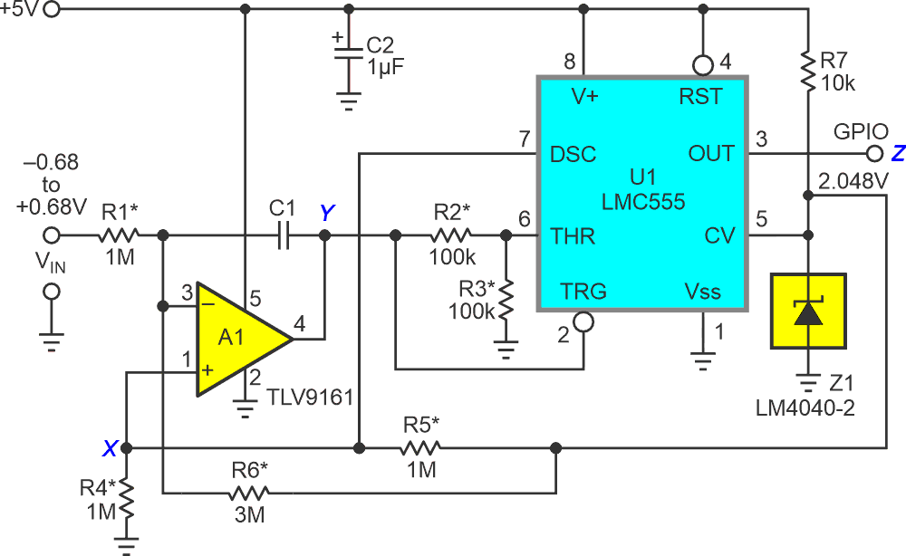
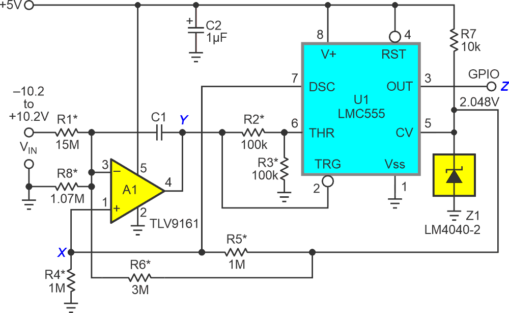
As Figure 1 shows, the design starts off with an old friend, the 555-analog timer.
 |
|
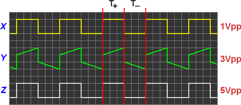
| Figure 1. | Op-amp A1 continuously integrates the incoming VIN signal, thus minimizing noise. Conversion occurs in alternating phases, T– and T+. The T–/T+ phase duration ratio is independent of the RC time constant, is therefore insensitive to C1 tolerance, and contains both VIN magnitude and polarity information. |
Incoming signal VIN is summed with the voltage at node X and accumulated by differential integrator A1. A conversion cycle begins when A1’s output (node Y) reaches 4.096 V and lifts timer U1’s threshold pin (THR) through the R2/R3 divider to the 2.048-V reference supplied by voltage reference Z1. This switches on U1’s DSC pin, grounding A1’s noninverting input through the R4/R5 divider, outputs a zero to the GPIO bit (node Z), and begins the T– phase as A1’s output ramps down. The duration of this T– phase is given by:
where VFS is the full scale voltage. The T– phase ends when A1’s output reaches U1’s trigger (TRG) voltage set to 1.024 V by Z1 and U1’s internal 2:1 divider. See the LMC555 datasheet for the gritty details.
This starts the T+ conversion phase with an output of one on the GPIO bit, and the release of DSC by U1, which drives A1’s noninverting input to 1.024 V, set by Z1 and the R4/R5 divider. The T+ positive-going ramp continues until A1’s output reaches the 4.096 VTHR threshold described above and initiates the next conversion cycle.
T+ phase duration is:
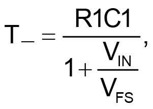
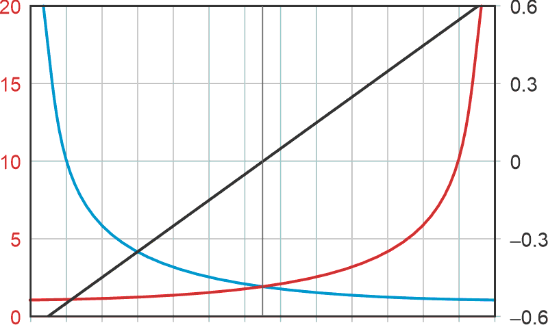
This frenetic frenzy of activity is summarized in Figure 2.
 |
|
| Figure 2. | Various conversion signals found at circuit nodes X, Y, and Z. |
Meanwhile, the GPIO pin is assumed to be connected to a suitable microcontroller counter/time peripheral that is accumulating T– and T+ durations for a chosen resolution and conversion rate. Something between 1 µs and 100 ns should work for the subsequent VIN calculation. This brings up that claim of immunity to integrator capacitor tolerance you might be wondering about.
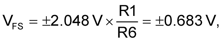
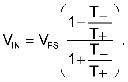
The durations of the T+ and T– ramps are proportional to C1, as shown in Figure 3.
 |
|
| Figure 3. | Black = VIN, Red = T+ duration in ms, Blue = T– duration, C1 = 0.001 µF. |
However, software arithmetic saves the day (and maybe even my reputation!) because recovery of VIN from the raw phase duration timeouts involves a bit of divide-and-conquer.
And, of course, when T– is divided by T+, the R1C1 terms conveniently disappear, taking sensitivity to C1 tolerance away with them!
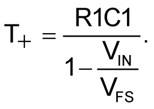
A final word about VFS. The ±0.683 V figure derived above is a minimum value, but any larger span can be easily accommodated by adding one resistor (R8) and changing another (R1). Here’s the scale-changing arithmetic:
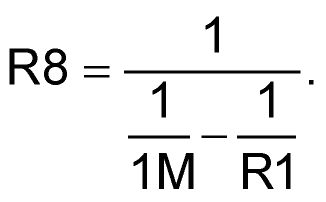
For example, ±10 V is illustrated in Figure 4.
 |
|
| Figure 4. | A ±10-V VIN span is easily accommodated – if you can find a 15 MΩ precision resistor. |
Note that R1 would probably need to be a series string to get to 15 MΩ using OTS resistors.