Ages ago, humankind crawled out of the primordial analog ooze and began to do digital. They soon noticed and quantified a fundamental need to interconnect their new quantized numerical novelties with the classic continuum of the ancestral engineer’s world. Thus arose the ADC.
Of course, there were (and are) an abundance of ADC schemes and schematics. One of the earliest and simplest of these was the single-slope type.
Single slope ADCs come in two savory flavors. In one, a linear analog voltage ramp is generated and compared to the input signal. The time required for the ramp to rise from zero (or near) to equality with the input is proportional to the input’s amplitude and taken as its digital conversion.
We recently saw an example contributed by Dr. Jordan Dimitrov to our own friendly Design Idea (DI) corner in “Voltage-to-period converter offers high linearity and fast operation” (Ref. 1).
In a different cultivar of the single sloper, a capacitor is charged to the input voltage, then linearly ramped down to zero. The time required to do that is proportional to VIN and counts (pun!) as the conversion result. An (extremely!) simple and cheap example of this type was published here about two and a half years ago in “A “free” ADC” {Ref. 2}
While simple and cheap are undeniably good things, too much of a good thing is sometimes not such a good thing. The circuit in Figure 1 adds a few refinements (and a bit more cost) to that basic design in pursuit of an order of magnitude (or two) better accuracy and perhaps a bit more speed.
 |
|
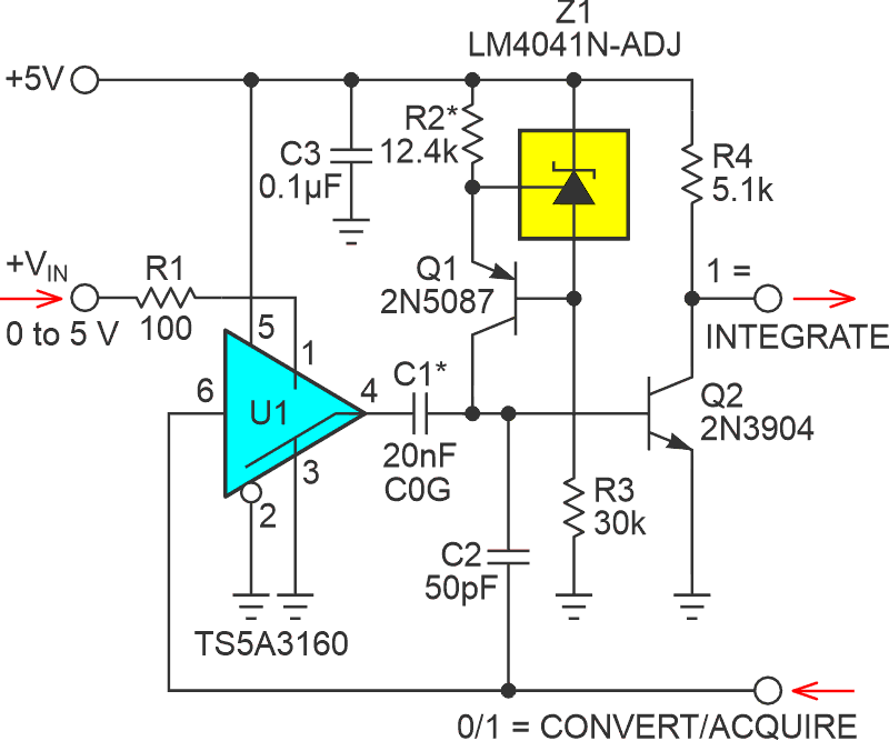
| Figure 1. | Simple speedy single-slope (SSSS) ADC biphasic conversion cycle. |
Here’s how it works:
- (CONVERT = 1) switch U1 charges C1 to VIN
- (CONVERT = 0) C1 is linearly discharged by 100 µA current sourced by Z1Q1
Note: Z1, C1, and R2 should be precision types.
Conversion occurs in two phases, selected by one GPIO bit configured for output (CONVERT/ACQUIRE).
During the ACQUIRE (1) interval SPDT switch U1 connects integrator capacitor C1 to the input source, charging it to VIN. The acquisition time constant of the charging is:
C1(R sZ1+ U1 RON, + Q2’s input impedance) = ~10 µs
To complete the charge to ½-lsb-precision at 12-bit resolution, this needs an ACQUIRE interval of:
10 µs × ln(212+1) = 90 µs.
The controlling microcontroller can then return CONVERT to zero, which switches the input side of C1 to ground, driving the base of the comparator transistor negative for a voltage step of –VIN, plus a “smidgen” (~12 mV).
This last is contributed by C2 to compensate for the zero offset that would otherwise accrue from Q2’s finite voltage gain and storage time.
Q1’s emergence from saturation drives INTEGRATE positive. Here it remains until the discharge of C1 is complete and Q1 turns back ON. This interval is:
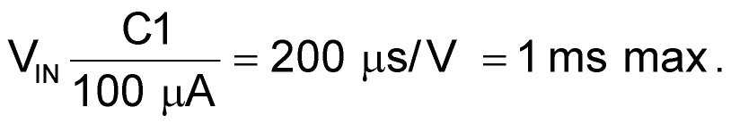
If the connected counter/peripheral runs at 20 MHz, then the max-count accumulation and conversion resolution will be 4000, or 11.97 bits.
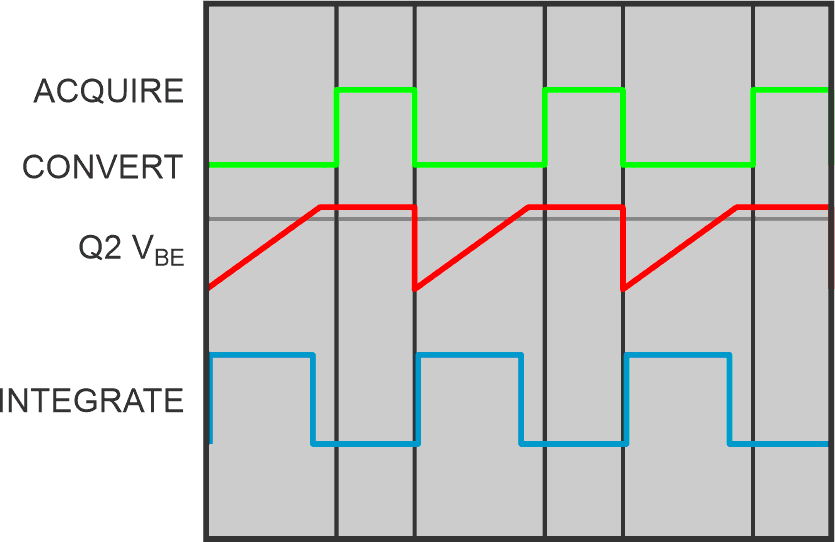
This 1-ms, or ~12-bit, conversion cycle is sketched in Figure 2. Note that good integral nonlinearity (INL) and differential nonlinearity (DNL) are inherent.
 |
|
| Figure 2. | The SSSS ADC waveshapes. The ACQUIRE duration (12 bits) is 90 µs. The INTEGRATE duration is 1 ms max (VIN·C1/IQ1 = 200 µs/V). Amplitude is 5 Vpp. |
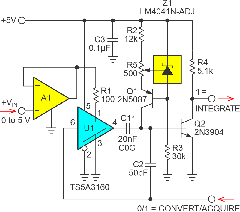
Of course, not all signal sources will gracefully tolerate the loading imposed by this conversion sequence, and not all applications will find the tolerance of available LM4041 references and R1C1 adequately precise.
Figure 3 shows fixes for both of these limitations. A typical RRIO CMOS amplifier for A1 eliminates the input loading problem, and the R5 trim provides a convenient means for improving conversion calibration.
 |
|
| Figure 3. | A1 input buffer unloads VIN, and R5 calibration trim improves accuracy. |
References
- Dimitrov, Jordan. "Voltage-to-period converter offers high linearity and fast operation."
- Woodward, Stephen. "A “free” ADC."