Simple analog circuits manage multi-PSU powerup and shutdown sequences
In projects containing digital and/or analog circuits, multiple power supplies are used, generally 5 V DC for digital circuits and 15 V DC for analog circuits. Some projects also use 24 V or 48 V DC as the third power supply. In many cases, these power supplies need to be switched on in sequence, commonly 5 V DC first and 15 V DC next, with a time delay in-between. Subsequently switching them off necessitates implementing this sequence in reverse, i.e., first in/last out (FILO) in total, with 15 VDC first and 5 V DC next and again with a time delay in-between.
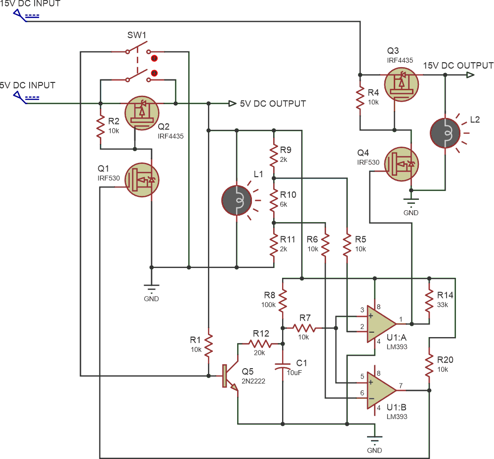
In MCU-based projects, this sequencing can be achieved through an appropriate software routine (Ref. 1). For non-MCU projects, conversely, Figure 1 shows a simple analog circuit that accomplishes this function for two power supplies/
 |
|
| Figure 1. | A simple analog circuit controls the powerup and shutdown sequencing of two power supplies. |
How does this circuit work? Fundamentally, it employs the charging and discharging of capacitor C1 to achieve both power supply sequencing and the interim time delay. SW1 is a two-pole ON/OFF switch. When it is pressed, 5 V is applied first through one pole and then through the second pole. 0 V applied to the base of Q5 creates an open circuit. Next, C1 gets charged through R8.
The voltage at C1 rises per the following formula:
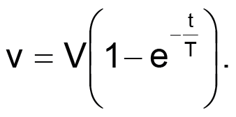
Here V = 5 V and T = R8 × C1. R9, R10 and R11 serve as voltage dividers to set the references for comparators U1B and U1A.
When the rising voltage v crosses through the first reference voltage set by R11, the U1B output goes HIGH, saturating Q1. This transition causes Q2 to conduct and connect to the 5 V output. Capacitor voltage v, further rising, next crosses through the second reference voltage set by R10 + R11. Now the U1A output goes HIGH, saturating Q4. Q3 now also conducts, with 15 V also made available at the output.
For switching off, although SW1 is now opened, 5 V initially continues to be fed to the output through the ongoing conduction of Q2. The base of Q5 goes HIGH, causing it to saturate. C1 resultantly starts discharging through R12. The voltage v at C1 decreases as per the formula:
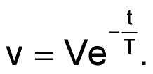
When this voltage goes below the reference voltage 2 set as the input to U1A, its output goes LOW. Q4 and Q3 now turn OFF. Hence, the 15 V DC output is switched OFF first. As the capacitor voltage further decreases with the passing of time, it goes below the reference 1 set at the input of U1B. Its output now also goes LOW, turning Q1 and Q2 OFF. The 5 V output, switched OFF last, implements the desired FILO sequence.
Notably, this design doesn’t employ a constantly power-consuming watchdog circuit. For different time delays, accordingly select R9, R10 and R11 to set the desired reference voltages. High current power supplies can be handled by using suitable MOS switches (Q2 and Q3).
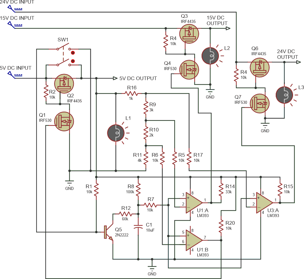
You can expand this concept to cover any number of power supplies to be operated in a time-delay FILO sequence. For example, Figure 2 shows a derived analog circuit, this time supporting three power supplies.
 |
|
| Figure 2. | An analog circuit derived from the previous one controls the powerup and shutdown sequencing of three power supplies, with the concept further as-needed expandable. |
Reference
- Ramalingam, Jayapal. "Short push, long push for sequential operation of multiple power supplies."