The iconic LM2917 tackles frequency-to-current conversion with (very) few externals.
Almost exactly 50 years ago – in June 1976, to be precise – National Semiconductor introduced the LM29x7 series, offering deceptively simple monolithic solutions to a frequently encountered signal processing problem: the flexible and accurate conversion of frequency into an analog signal. I say “deceptively simple” because actually, these chips are very capable interfaces with versatile inputs, internal active zener voltage references (with the LM2917), and a configurable output that includes an opamp-driven uncommitted Darlington transistor.
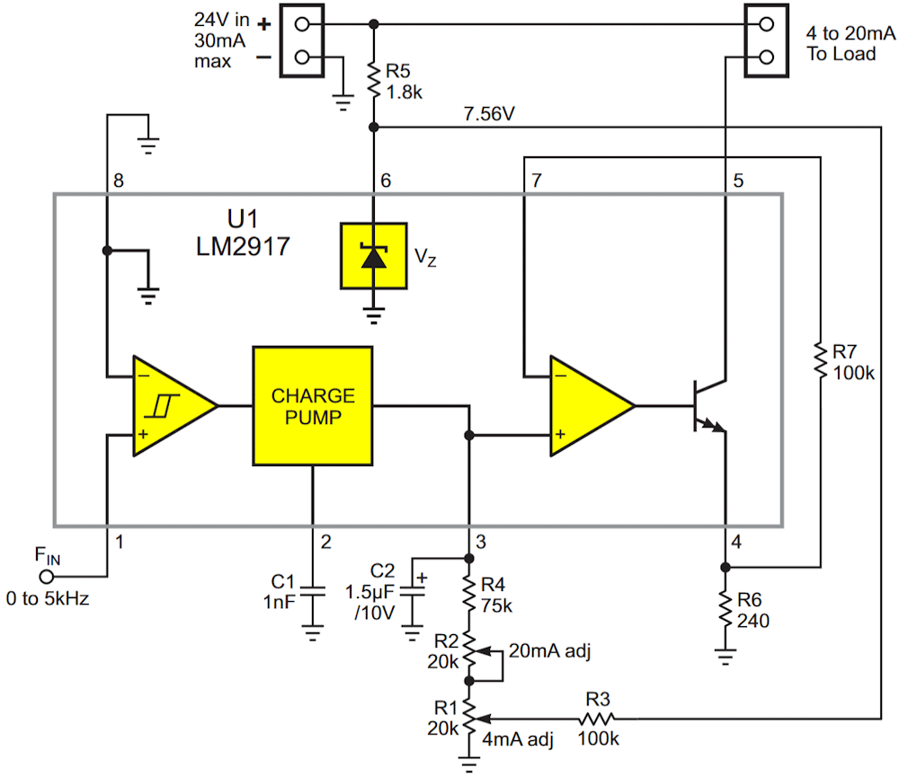
Although initially targeted at automotive applications, the LM29x7 series’ flexibility makes them highly handy in other contexts, including industrial applications like monitoring turbine-type flow meter flow rate and small motor tachometry. Figure 1’s facile conversion of a frequency input to a universal 4-20 mA current loop format shows how minimalist – it makes do with just nine paltry passives – such a circuit can be when implemented with a LM2917.
 |
|
| Figure 1. | A 2917 with internal voltage reference converts a 0-5 kHz input to a 4-20 mA output. Single-pass calibration of both ends of the output span is available. First step: input 0 Hz and adjust R1 for 4 mA output. Second step: input 5 kHz and adjust R2 for 20 mA. Third step: there is no third step. You’re done. |
Here’s how it works.
Incoming pulses are converted by the internal Schmidt trigger comparator and charge pump into constant-current (180 µA) pulses delivered to pin 3. Each pulse cycle carries a charge quantum QP = VZ C1 so that the average current out of pin 3 as a function of the Finput frequency is I3 = FIN·QP = FIN·VZ·C1. For the values shown, that works out to I3 = 7.56 µA/kHz = 0 to 38 µA as FIN goes from 0 to 5 kHz. For calibration stability, C1 should be a temperature-stable type like C0G.
The R1…R4 resistor network hung from pin 3 converts this 0 to 38 µA to 0 to 4 V which is added to a 1 V offset supplied by R3. The resulting 1 to 5 V total is converted by the internal output opamp and Darlington via current sense R6 to the final 4 to 20 mA output. R7 provides some bias current cancellation, which is useful since the thirsty opamp inputs can draw as much a 500 nA. If uncorrected, that could create a 50 mV voltage offset error on pin 3. Meanwhile, C2 provides ripple-suppression filtering.
However, none of this explains why R1 and R2 are variable. Here’s why. Although U1’s spec’d linearity and temperature coefficient are good, its initial tolerances aren’t so great: about ±10%. See “gain constant K” in Table 7.5 here (PDF). Therefore some post-assembly final calibration is pretty much unavoidable, which is the purpose of R1’s (4 mA zero) and R2’s (20 mA full-scale 5 kHz) tweakability. But at least if you do the adjustments in the right order (first R1, then R2), they won’t interact and calibration can be completed in s single pass.
So it shouldn’t Hz too much. (No such promises for his jokes, however! Ed.)