When analog circuits mix with digital, the former are sometimes dissatisfied with the latter’s usual single supply rail. This creates a need for additional, often negative polarity, voltage sources that are commonly provided by capacitive charge pumps.
The simplest type is the diode pump, consisting of just two diodes and two capacitors. But it has the inherent disadvantages of needing a separately sourced square wave to drive it and of producing an output voltage magnitude that’s at least two diode drops less than the supply rail.
Active charge pump switches (typically CMOS FETs) are required to avoid that.
Many CMOS charge pump chips are available off the shelf. Examples include the multi-sourced ICL7660 and the Maxim MAX1673 pumps that serve well in applications where the current load isn’t too heavy. But they aren’t always particularly cheap (the 1673 for example is > $5 in singles) and besides, sometimes the designer just feels the call to roll their own. Illustrated here is an example of the peculiar outcomes that can happen when that temptation isn’t resisted.
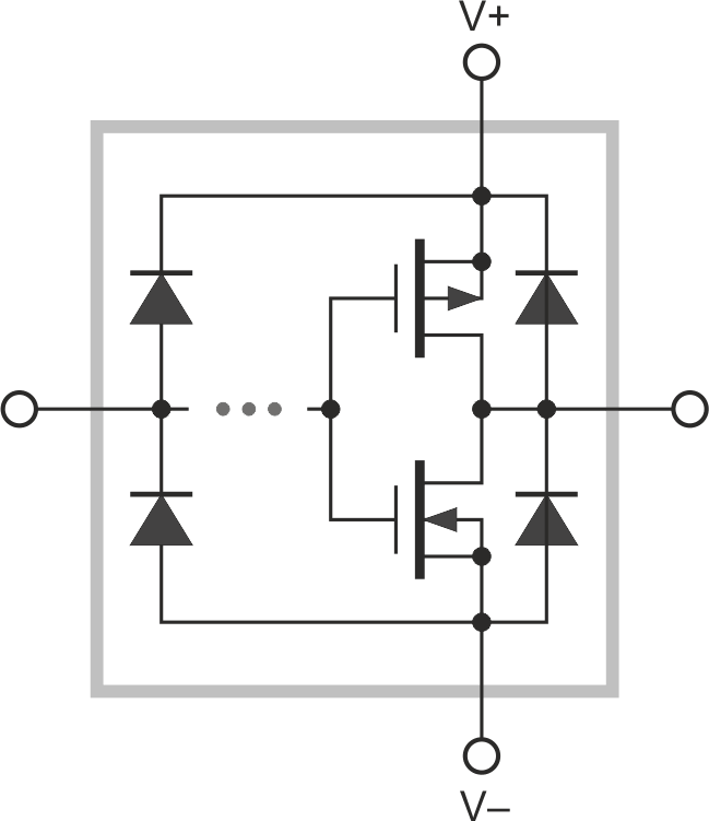
The saga begins with Figure 1, showing a (vastly simplified) sketch of a CMOS logic inverter.
 |
|
| Figure 1. | Simplified schema of typical basic CMOS gate I/O circuitry showing clamping diodes and complementary FET switch pair. |
Notice first the input and output clamping diodes. These are included mainly to protect the chip from ESD damage, but a diode is a diode and can therefore perform other useful functions, too. Similarly, the P-channel FET pair was intended to connect the V+ rail to the output pin when outputting a logic ONE, and the N-channel for connection to V- to pin for a ZERO. But CMOS FETs will willingly conduct current in either direction when ON. Thus, current running from pin to rail works just as well as from rail to pin.
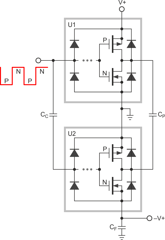
Figure 2 shows how these basic CMOS facts relate to charge pumping and voltage inversion.
 |
|
| Figure 2. | Simplified topology of logic gates comprising voltage inverter, showing driver device (U1), switch device (U2), and coupling (CC), pump (CP), and filter (CF) capacitors. |
Imagine two inverters interconnected as shown in Figure 2 with a square wave control signal coupled directly to U1’s input and through DC blocking cap CC to U2’s with U2’s input clamps providing DC restoration.
Consider the ZERO state half cycle of the square wave. Both U1 and U2 P-channel FETs will turn on, connecting the U1 end of CP to V+ and the U2 end to ground. This will charge CP with its U1 terminal at V+ and its U2 end at ground. Note the reversed polarity of current flow into U2’s output pin due to CP driving the pin positive and from there to ground through U2’s P FET and positive rail pin.
Then consider what happens when the control signal reverses to the ONE state.
Now the P FETs will turn OFF while the N FETs turn ON. This forces the charge previously accepted by CP to be dumped to ground through U1 and its complement drawn from U2’s V- pin, thus completing a charge-pumping cycle that delivers a quantum of negative charge:
Q- = –(CPV+ + CFV-)
to be deposited on CF. Note that reversed current flow through U2 occurs again. This cycle will repeat with the next reversal of the control signal, and so on, etc., etc.
During startup, until sufficient voltage accumulates on CF for normal operation of internal gate circuitry and FET gate drive, U2 clamp diodes serve to rectify the CP drive signal and charge CF.
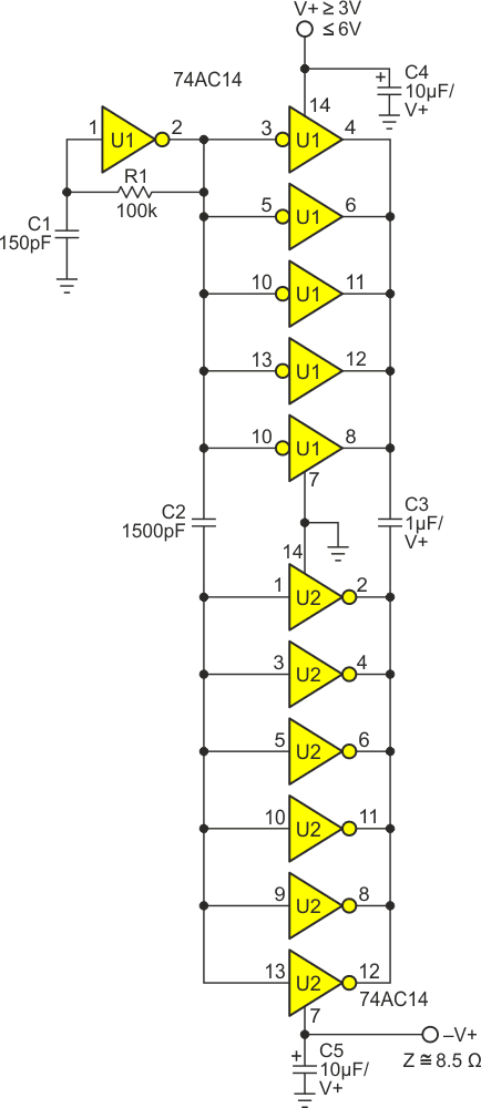
That’s the theory. Translation of Figure 2 into practice as a complete voltage inverter is shown in Figure 3. It’s really not as complicated as it looks.
 |
|
| Figure 3. | Complete voltage inverter: 100 kHz pump clock (set by R1C1), Schmidt trigger and driver (U1), and commutator (U2). |
A 100 kHz pump clock is output on pin 2 of 74AC14 Schmidt trigger U1. This signal is routed to the five remaining gates of U1 and the six gates of U2 (via coupling cap C2). Negative charge transfer occurs through C3 into U2 and accumulates on filter cap C5.
Even though the Schmidt hysteresis feature isn’t really needed for U2, the same type is used for both chips to improve efficiency-promoting synchronicity of charge-pump switching.
Some performance specs (V+ = 5 V):
- Impedance of V- output: 8.5 Ω
- Maximum continuous load: 50 mA
- Efficiency at 50 mA load: 92%
- Efficiency at 25 mA load: 95%
- Unloaded power consumption: 440 µW
- Startup time < 1 millisecond
But finally, is there a cost advantage to rolling your own? Well, in singles, the 1673 is $5, the 7660 about $2, but two 74AC14s can be had for only a buck. The cost of passive components is similar, but this DI circuit has more solder joints and occupies more board area. So, the bottom line…??
But at least using outputs as inputs and ground as an output was fun.
And an afterthought: For higher voltage operation, simply drop in CD40106B metal-gate chips for the 74AC14s, then with no other changes, V+ and V- can be as high as 20 V.