Avoiding op-amp output saturation error by keeping op-amp outputs “live” and below zero volts is a job where a few milliamps and volts (or even fractions of one volt) of regulated negative rail can be key to achieving accurate analog performance. The need for voltage regulation arises because the sum of positive and negative rail voltages mustn’t exceed the recommended limits of circuit components (e.g., only 5.5 V for the TLV9064 op-amp shown in Figure 1). Unregulated inverters may have the potential (no pun!) to overvoltage sensitive parts and therefore may not be suitable.
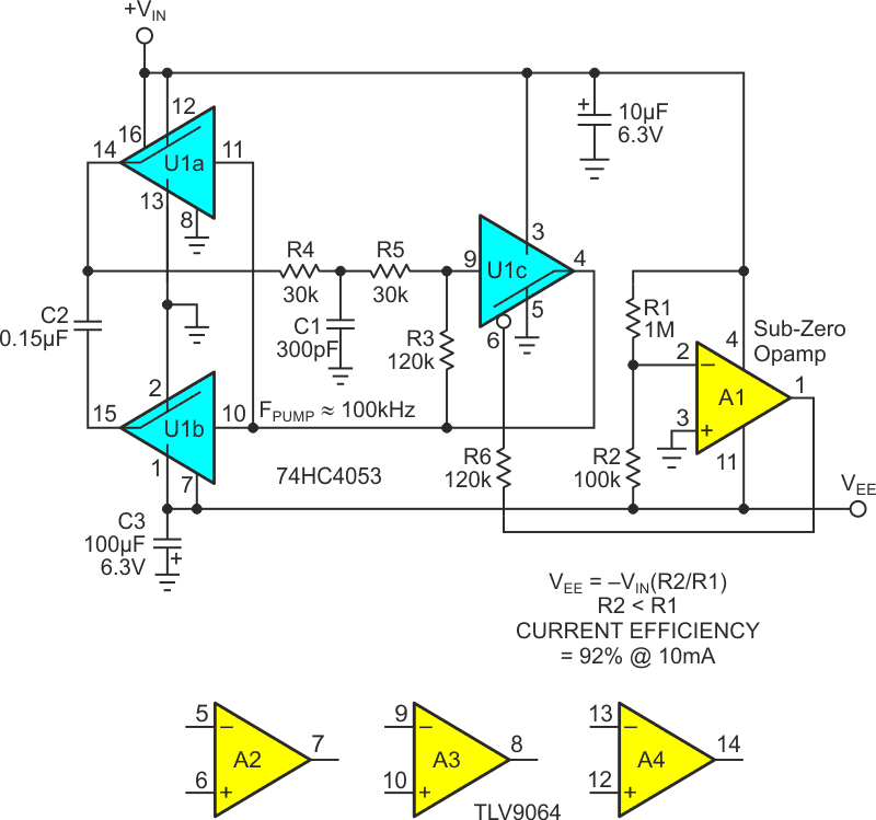
Figure 1 shows the circuit: A simple regulated charge pump inverter based on the venerable and versatile HC4053 triple SPDT CMOS switch and most any low power RRIO op-amp. It efficiently and accurately inverts a positive voltage rail, generating a programmable negative output that’s regulated to a constant fraction of the positive rail. With VIN = 5 V, its output is good for currents from zero up to nearly 20 mA, the upper limit depending on the VEE level chosen by the R1:R2 ratio. It’s also cheap with a cost that’s competitive with less versatile devices like the LM7705. It’s almost unique in being programmable for outputs as near zero as you like, simply set by the choice for R2.
 |
|
| Figure 1. | U1 makes an efficient charge pump voltage inverter with comparator op-amp A1 providing programmable regulation. |
But enough sales pitch. Here’s how it works.
U1a and U1b act in combination with C2 to form an inverting flying-capacitor pump that transfers negative charge to filter capacitor C3 to maintain a constant VEE output controlled by A1. Charge pumping occurs in a cycle that begins with C2 being charged to VIN via U1a, then completes by partially discharging C2 into C3 via U1b. Pump frequency is roughly 100 kHz under control of the U1c Schmidt trigger style oscillator, so that a transfer occurs every 10 µs. Note the positive feedback around U1c via R3 and inverse feedback via R4, R5, and C1.
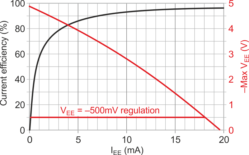
Figure 2 shows performance under load with the R2:R1 ratio shown.
 |
|
| Figure 2. | Output voltage and current conversion efficiency vs output current for +VIN = 5 V. |
No-load current draw is less than 1 mA, divided between U1 and A1, with A1 taking the lion’s share. If VEE is lightly loaded, it can approach –VIN until A1’s regulation setpoint
kicks in. Under load, Max VEE will decline at ~160 mV/mA but VEE remains rock solid so long as the VEE setpoint is at least slightly less negative than Max VEE.
A word about “bootstrapping”: Switch U1b needs to handle negative voltages but the HC4053 datasheet tells us this can’t work unless the chip is supplied with a negative input at pin 7. So U1’s first task is to supply (bootstrap) a negative supply for itself by the connection of pin 7 to VEE.
“Sub-zero” comparator op-amp A1 maintains

via negative feedback through R6 to U1 pin 6 Enable. When VEE is more positive than the setpoint, A1 pulls pin 6 low, enabling the charge pump U1c oscillator and the charging of C3. Contrariwise, VEE at setpoint causes A1 to drive pin 6 high, disabling the pump. When pin 6 is high, all U1’s switches open, isolating C2 and conserving residual charge for subsequent pump cycles. R6 limits pin 6 current when VEE < –0.5 V.
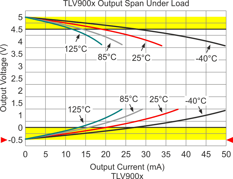
Figure 3 shows how a –500-mV sub-zero negative rail can enable typical low-voltage op-amps (e.g., TLV900x) to avoid saturation at zero over the full span of rated operating temperature for output currents up to 10 mA and beyond. Less voltage or less current capability might compromise accurate analog performance.
 |
|
| Figure 3. | VEE = –500 mV is ideal for avoiding amplifier saturation without overvoltaging LV op-amps. |
U1’s switches are break-before-make, which helps both with pump efficiency and with minimizing VEE noise, but C3 should be a low ESR type to keep the 100 kHz ripple low (about 1 mVpp @ IEE = 10 mA). You can also add a low inductance ceramic in parallel with C3 if high frequency spikes are a concern.
Footnote: I’ve relied on the 4053 in scores of designs over more than a score of years, but this circuit is the very first time I ever found a practical use for pin 6 (/ENABLE). Learn something new every day!