In the first part (Ref. 1) of this Design Idea, we saw how a cheap op-amp can give remarkably precise readings from an RTD. We also found that it was a false economy, owing to incurable thermal drift. This concluding part fixes that problem by using a more costly OP177 precision op-amp, which is still much cheaper than an RTD sensor alone.
 |
|
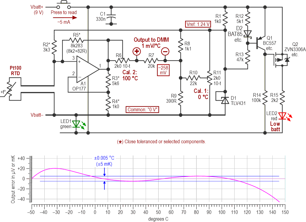
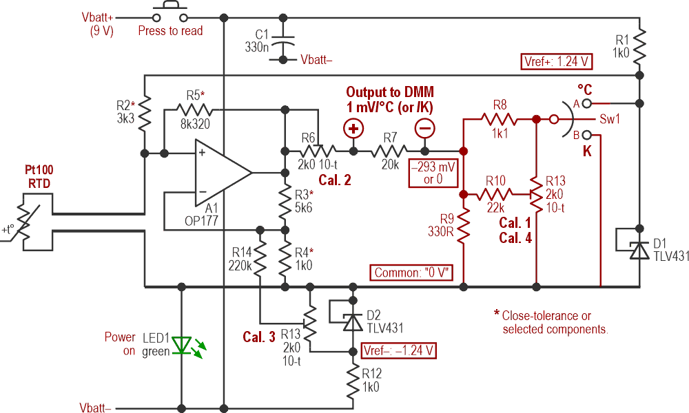
| Figure 1. | Using a precision op-amp lets us set the output reference level with a passive network because thermal drifts and mismatches are no longer a problem. LED1 acts both as a rail-splitter and a power indicator, while LED2 gives a simple low-battery warning. The calculated error curve assumes perfect components and shows the limits to precision for this circuit. |
Now that we don’t need to worry about drift, we can balance the output of the input stage against a passive network: R8 to R11 in Figure 1. That figure also shows the (ideal, theoretical) error curve once the positive-feedback resistor R5 has been trimmed for minimum errors around 0 to 100 °C, which is the same as part 1’s Figure 2.
 |
|
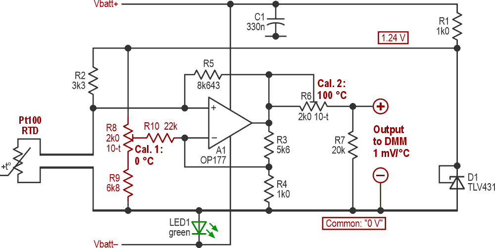
| Figure 2. | Adding a biasing network to A1 allows its output to be at 0 mV (common) when sensing 0 °C, and to swing negative for lower temperatures. |
While this performs identically to part 1’s circuit, there are some practical differences. The OP177 needs at least a 6 V rail to work (but can handle ±15 V), so a 9 V battery (e.g., MN1604) makes a good power source. The rail must be split, which is where LED1 comes in. R1 passes current through the voltage reference D1 and the components bridging it. That current fed through LED1 both lights it and offsets the common rail by a couple of volts from the negative one, which is plenty considering the small voltage swings involved. Bright, pure green devices dropped about 2.3 V; normal ones gave less but were rather dim. R1 was chosen to guarantee the correct operation of D1 down to a battery voltage below 5.6 V, which was where my op-amps actually failed.
Flat battery: you will be warned
The other addition (R12–15, Q1/2, LED2) should ensure that you never run the battery that far down! It’s a simple low-battery indicator that lights LED2 when the voltage across R1 falls below a critical level. As built, that tripped when the battery fell to ~6.5 V. A suitable micropower comparator – didn’t have one handy – would have been neater and not temperature-sensitive, though D2 helps with that. This circuit block isn’t shown on subsequent schematics, but could easily be added.
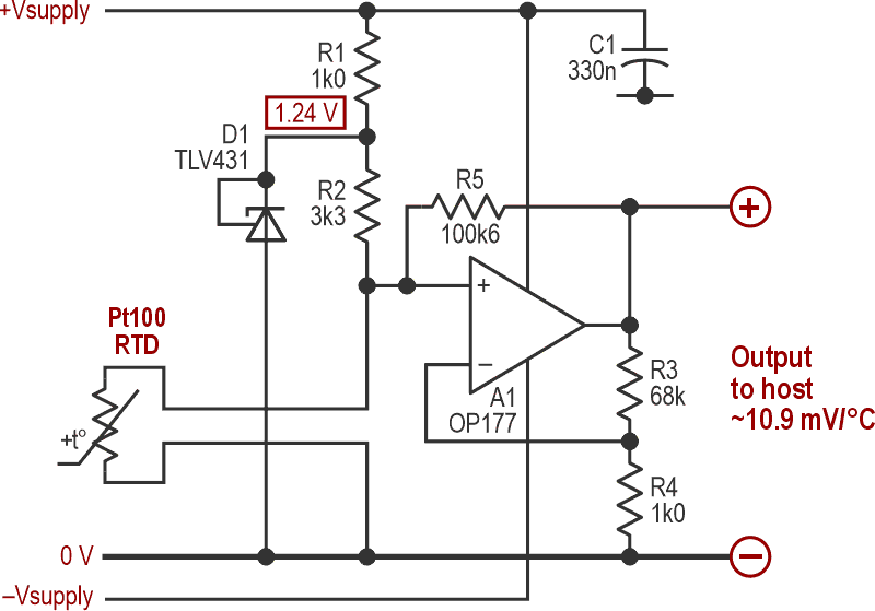
Next question: since we now have split rails, why not bias A1 with an offset so that its output refers to the common rail, giving 0 V at 0 °C? It’s more elegant, because “negative” temperatures now give a negative output, it saves a resistor (cheapskate), and is shown in Figure 2. But that passive network, though discarded for now, will come in handy later.
The necessary biasing is provided by R8–10. Because R4 is now bridged by ~23k, A1’s gain is increased slightly. R5’s new value gives the same error performance as before.
Increasing the measurement span
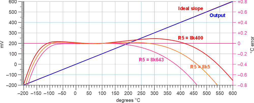
So far, we’ve only looked at a comparatively narrow temperature band. Taking that to extremes is instructive. Figure 3 plots the errors from –200 up to +600 °C. (The Callender-Van Dusen equations apply up to 661 °C – the melting point of aluminum.) At the end of part 1, we saw that R5 determines the errors. Now, we can see how varying it can give a different balance of errors over a wider span. Figure 3’s plots are normalized for zero error at 0 and 100 °C, which are still valid as calibration points and are used to calculate the ideal slope. No components apart from R5 are affected, though the settings of R6 and R8 will change.
 |
|
| Figure 3. | Plotting the errors for various values of R5 – the positive feedback resistor – shows that we can optimize performance for minimal errors around 0–100 °C (magenta) or accept a wider error band over a greater temperature range. The red curve is within 0.1 °C from –130 to +420 °C and 1 °C from < –200 to >+640 °C. |
Indicating in Fahrenheit
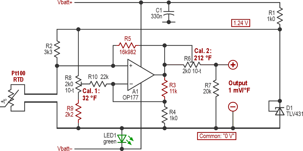
With a few changes, Figure 2’s circuit can give a direct 1 mV/°F reading, should you need that. The gain must be increased by a nominal 9/5 and an extra offset of 32° provided. Figure 4 shows what’s needed.
 |
|
| Figure 4. | Changing three components gives an output of 1 mV/°Fahrenheit. |
This works well, but needs care in calibration. Using the 100/138.5 Ω (0/100 °C) RTD sim from part 1 would mean some iteration: set 32 °F, set 212 °F, and repeat… Paralleling the 100 Ω resistor with 1k3354 drops it to 93.0334 Ω, the resistance of a (theoretically perfect) 100Ω-PtRTD at 0 °F or –17.7778 °C. (Yes, more decimals than you’ll need; it never hurts.) The sim then switches cleanly between 0 and +179.0 °F – not 180°, because of the RTD’s response curve, which also introduces a minute error at the low point. Hopefully, the actual RTD will be precise enough to minimize the time spent with crushed ice and condensing steam needed for the final trim.
Kelvins
Figure 1’s circuit gives an output (from A1) of ~260 mV at 0 °C. If the RTD’s curve were linear and A1’s gain ideal, that would be 273.15 mV, the final readout still being at 1 mV/K. Applying a small offset to A1 fixes things so that we can read absolute temperatures directly. Figure 5 details the necessary changes, with the offset coming indirectly from the voltage across LED1. Again, R5 is shown trimmed for maximum accuracy in the 273.15–373.15K region – and those values are what your meter must show in millivolts when using the 100/138.5 Ω sim gadget.
 |
|
| Figure 5. | A small negative offset allows the basic circuit to give an output directly proportional to absolute temperature. |
Something simple, with split supplies
A final version of the circuit can eliminate the DMM. OP177s will run on supplies from 6 to >30 V, so should you need to add an RTD to kit having suitably split rails, Figure 6 – the simplest variant, and little more than part 1’s figure 1 made practical – may be ideal.
 |
|
| Figure 6. | Stripping out all the frills and fancies leaves a basic circuit that is ideal for running off split rails and compatible with most ADCs. |
R3 is now increased to 68k for a gain of ~69, giving ~10.9 mV/°C, R5 being adjusted accordingly. The 0 °C datum is now at ~2.43 V, so even with ±5 V rails, readings can span from –120 to +150 °C (±0.1 °C error) before A1 saturates. A higher positive rail would allow far higher temperature readings; the lower limit – always above zero volts – merely depends on the allowable error at that point.
This assumes that the output will be read directly by an ADC, probably using a 5 V reference, and that the host system can adjust the zero and the span, which is why no calibration trimmers are shown: that host needs only simple arithmetic rather than the math of a full CVD calculation. For different spans, try the equations for calculating R5 as shown at the end of part 1.
The final build
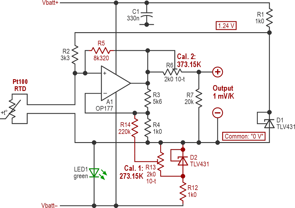
These circuits were all breadboarded and checked, but I ended up building something slightly different for actual use (Figure 7). This variant starts with the Kelvin approach and then adds the passive reference network discarded from Figure 1, allowing instant switching between the two temperature scales.
 |
|
| Figure 7. | Referring the output from the amplifying stage to either a positive reference or to common allows the indication to be switched between Celsius and Kelvin. |
For readings in Celsius, the reference network is fed from VREF; for Kelvins, the top of the network is grounded, which both zeroes the reference and keeps the extra resistance seen by R10 constant. This may or may not be useful because on most DMMs the Kelvin range will lose a decimal point compared with the Celsius, so that reading in °C and adding 273.15 gives better accuracy, but it was a fun thing to try.
No DMMs were harmed in the making of this DI.
References
- Cornford, Nick. "Newer, shinier DMM RTDs – part 1."