Introduction
Electronic equipment uses predominantly positive voltage rails for power. Occasionally, some negative voltage rails are also used. For this reason, negative (or inverting) output DC/DC converter solutions are not as common as their positive output DC/DC counterparts. Nevertheless, when powering high performance devices in factory automation, building automation, and communications systems such as high speed DACs, op amps, RF power amplifiers, AFEs, GaN FET gate drivers, IGBT gate drivers, etc., a negative voltage rail is needed. Designers face a big challenge looking for a negative voltage solution where most legacy devices require external level shifter circuits with which to communicate. They are also outdated, inefficient, complex, and bulky. This article discusses in detail the drawbacks of legacy solutions, and then investigates a new breed of highly integrated devices that addresses the deficiency, and offers a compact, easy to use, and highly efficient negative output DC/DC solution.
The negative output DC/DC converter challenges
A typical power system has its lowest voltage potential as ground reference, or GND. For a positive output DC/DC output converter, the ground reference is simply the GND (0 V potential). Its input/output signals are naturally referenced to this ground. The system controller communicates with the DC/DC converter simply and directly to those I/O pins. Figure 1 illustrates such a system where the system microcontroller drives the EN (enable) pin of the converter to turn it on and off. The controller also reads the status of the converter through its PGOOD (that is, RESET) pin to know whether the converter power output is within its regulation and is ready for powering up the whole system. For simplicity, only one DC/DC converter is shown here, but the principle also applies to systems with multiple positive voltage rails.
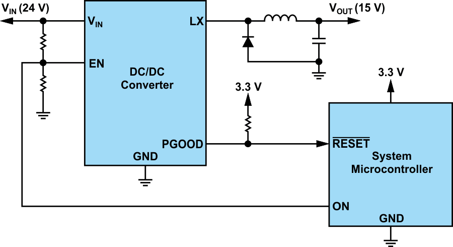 |
|
| Figure 1. | Example of a simplified schematic of a system using solely positive voltage rails. |
When a negative DC/DC converter is used, communication to the system controller is not trivial. The converter has its I/O pin referenced to its lowest voltage potential, which in this case is the negative output voltage, not the system GND. When using negative voltage rails, designers need to implement level shifter circuits for the system microcontroller to communicate with the DC/DC converter. Figure 2 illustrates a simplified schematic of a system with two level shifters.
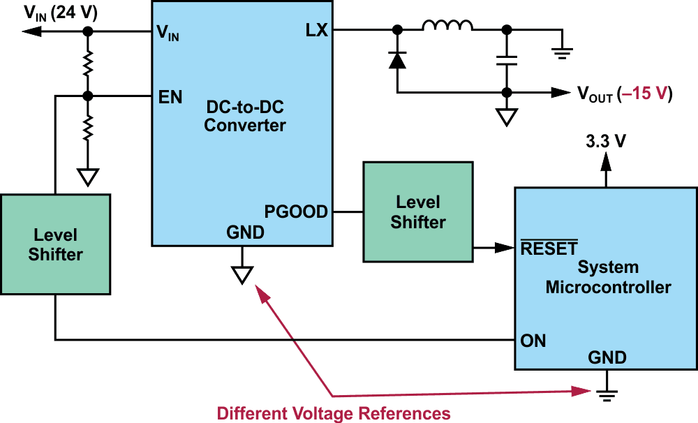 |
|
| Figure 2. | Example of a simplified schematic of a system using negative voltage rails. |
Again, for simplicity, only one negative output DC/DC converter is shown here. But the principle applies to system with multiple negative voltage rails or with a mix of both positive and negative voltage rails. One level shifter is needed per each I/O pin of each negative output DC/DC converter.
The level shifter circuit is large, creating a challenge for the designers. In addition, legacy negative DC/DC converter solutions are complex and inefficient, imposing yet another challenge.
Challenge 1: level shifter
Figure 3 illustrates a typical level shifter circuit. Its purpose is to shift the ground reference of a signal to match that of the system microcontroller. It is used here to translate the ON command from the system microcontroller to turn on/off the DC/DC converter. This level shifter consists of nine components. Its operation is straightforward: when ON is driven high by the system controller, Q1 turns on, which in turn biases Q2 on and drives EN high to enable the DC/DC converter. When ON is driven low, both Q1 and Q2 are off and EN is driven low to disable the converter.
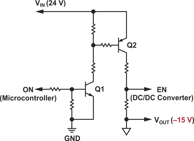 |
|
| Figure 3. | The typical level shifter circuit translates the ON command from the system controller. |
Figure 4 describes a common level-shifter circuit variation. It is used here to translate the PGOOD signal from the DC/DC converter so that the system microcontroller can read. When PGOOD is driven high (open drained) by the DC/DC converter, Q3 turns on, which in turn biases on Q4 and drives RESET high, taking the system microcontroller out of reset.
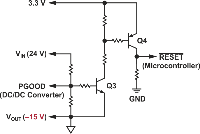 |
|
| Figure 4. | A level shifter translates the PGOOD signal from the DC/DC converter. |
These 2 level shifters require 18 external components, imposing a challenge to the designers trying to fit the solution to the ever-shrinking equipment and board space.
Challenge 2: inefficiency
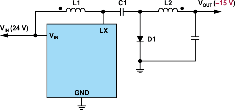
The legacy negative output DC/DC solution is inefficient. The extra heat generated due to inefficiency creates another challenge for designers, who now have the extra burden of removing that heat from the system. Figure 5 shows a simplified circuit schematic of such a system.
 |
|
| Figure 5. | A simplified schematic of a nonsynchronous, dual-inductor inverting output DC/DC converter. |
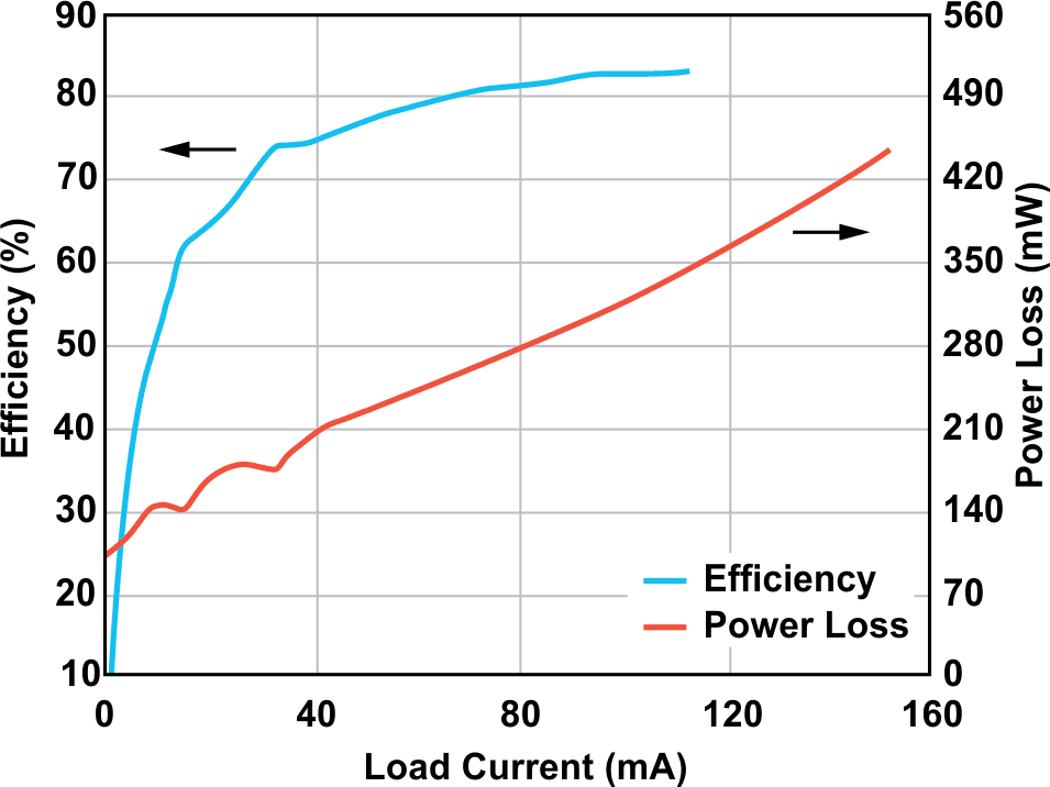
This topology faces two inefficiency issues. First, it employs nonsynchronous switching where the output rectifying diode, D1, dissipates more power compared to a synchronous solution. Second, it has an extra power inductor, L1, and an extra capacitor, C1, which also dissipate more power. Figure 6 shows the efficiency curve for this converter, measured at +12 V input and –15 V output. Its peak efficiency is only 83% while dissipating approximately 460 mW at 150 mA output current.
 |
|
| Figure 6. | The power loss curve shows the efficiency of a nonsynchronous, dual-inductor inverting output DC/DC converter. |
Smaller, more efficient negative output DC/DC solution
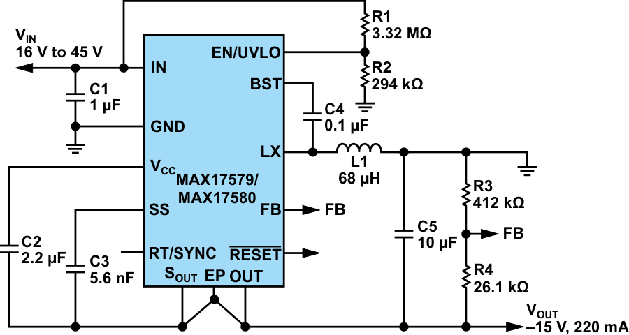
The MAX17577 and MAX17578 were developed to meet the growing requirements for smaller solution size and lower heat generating devices in factory automation, building automation, and communications systems. The devices integrate level shifting circuitry to reduce component cost and count, and they employ synchronous rectification for the best efficiency. These are the industry’s smallest and highest efficiency synchronous inverting DC/DC step-down converters. Figure 7 shows their typical application circuit.
 |
|
| Figure 7. | Highly integrated, most efficient negative output DC/DC converter. |
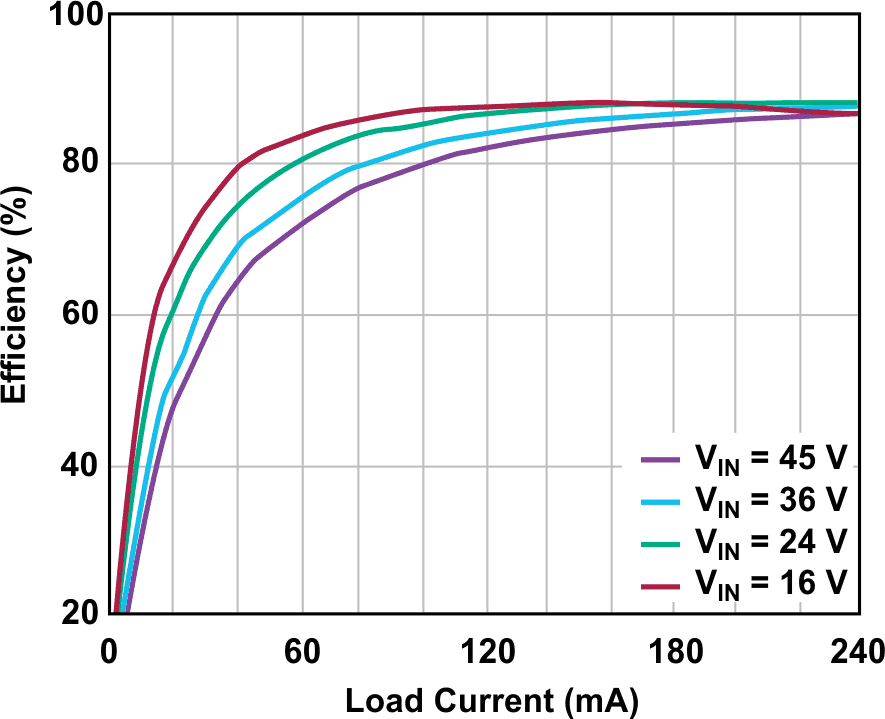
The MAX17577 and MAX17580 have a wide input voltage range. The devices operate from 4.5 V to 60 V input and can deliver up to 300 mA output current. With integrated level shifters, these devices conserve up to 72% of board space by reducing component count by half while using 35% less energy than the closest legacy solution. Figure 8 shows MAX17577’s peak efficiency at 88.5%, measured at 16 V input and –15 V/150 mA output. This is 5.5% points of higher efficiency comparing to the legacy solution shown in Figure 6. Why is efficiency important? At 88.5% efficiency, the device dissipates only 292 mW while delivering 2.25 W power to the load. 292 mW means 37% less heat for the system to cool compared to the 460 mW amount of the legacy solution shown earlier.
 |
|
| Figure 8. | MAX17579’s efficiency at –15 V output. |
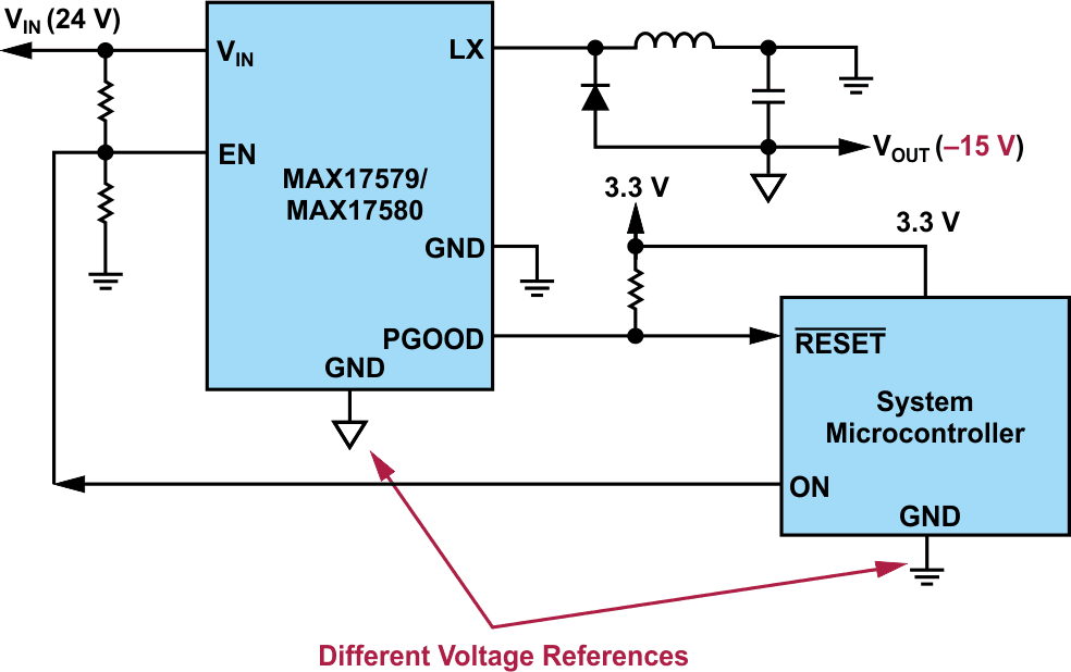
Figure 9 shows an improved version of Figure 2, eliminating the level shifters. The system microcontroller can communicate directly with MAX17579/MAX17580 even though they have different grounding references.
 |
|
| Figure 9. | The MAX17579/MAX17580 in a system using negative voltage rails. |
It is also worth noting that with a wide operating voltage range, these new solutions can withstand and tolerate system voltage fluctuations such as power surge event, back EMF and cable voltage ringing, etc. and increase system reliability. In addition, there are the MAX17577 and MAX17578, which are in the same family with similar performance, but can deliver up to 1 A of output current. These devices are great for powering RF power amplifiers, GaN FET gate drivers, IGBT gate drivers, etc.
Conclusion
Growing requirements for smaller solution size and lower heat generation in devices in factory automation, building automation, and communications systems impose big challenges for designers looking for negative voltage DC/DC converters where most legacy solutions are outdated, inefficient, complex, and bulky. A new breed of highly integrated devices with onboard level shifters, synchronous rectification, and a wide operating input voltage brings to the table the most compact, highly efficient, and robust negative output DC/DC solutions.
Materials on the topic
- Datasheet Maxim MAX17577
- Datasheet Maxim MAX17580